PUBLISHER: Mordor Intelligence | PRODUCT CODE: 2187318

PUBLISHER: Mordor Intelligence | PRODUCT CODE: 2187318
Indium Phosphide Wafer - Market Share Analysis, Industry Trends & Statistics, Growth Forecasts (2027 - 2032)
According to Mordor Intelligence, the indium phosphide wafer market size is expected to increase from USD 221.4 million in 2026 to USD 247.4 million in 2027 and reach USD 438.5 million by 2032, growing at a CAGR of 12.13% over 2027-2032.
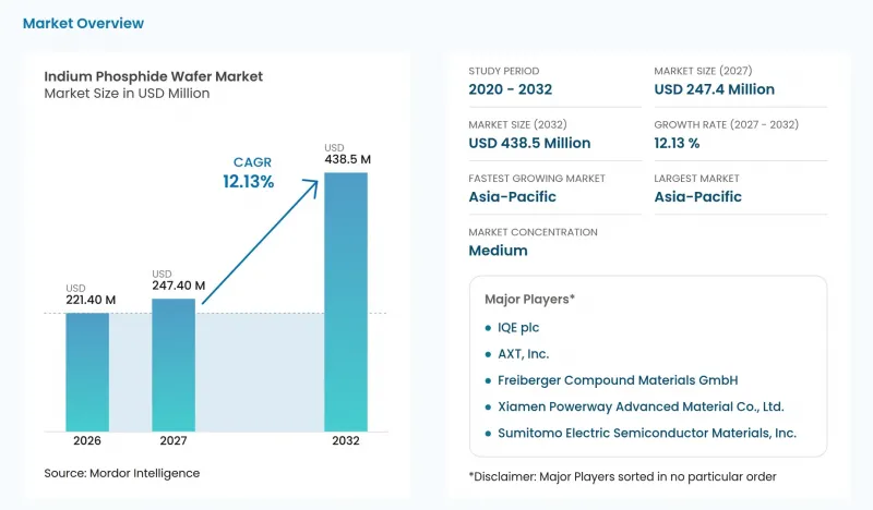
This report is segmented by Diameter (100 mm and more), Wafer Doping Type (Undoped Conductive and more), Application (Photonics and Optical Transceivers and more), End-user Industry (Telecommunications and Datacom and more), Manufacturing Technology (VGF-grown Bulk Wafers and more), and Geography. The market forecasts are provided in terms of value (USD), based on availability.
Global Indium Phosphide Wafer Market Trends and Insights
High-speed optical transceiver demand (400G/800G/1.6T)
High-speed optical links increase the need for InP devices and the wafer processing required to produce them. In March 2026, Coherent said demand for InP devices, including electro-absorption modulated lasers (EMLs) used in 800G to 6.4T transceivers, was driving expansion of its internal wafer-fab capacity. In August 2026, the company said data-center demand was driving growth acceleration and that it was on track to double internal InP output by year-end 2026 and more than double it again by 2027. Its March expansion involved ramping 6-inch capacity in Texas and Sweden and adding it in Switzerland. Meeting those output targets would require sustained substrate processing inside its fabs, translating optical demand into a manufacturing-throughput requirement.
5G backhaul infrastructure rollout and emerging 6G backhaul planning
Backhaul creates distinct opportunities in leased-fiber services and the optical interfaces planned for future networks. In May 2025, U Mobile appointed Telekom Malaysia to provide leased-fiber backhaul for its nationwide Malaysian 5G rollout. By October 6, 2026, U Mobile reported 90% coverage of populated areas nationwide. The International Telecommunication Union's Telecommunication Standardization Sector (ITU-T) identified 800GE/1.6TE backhaul interfaces among IMT-2030 optical-network technologies in its October 2025 GSTR-ION-2030 report. Separately, ITU released its ION-2030 framework in February 2026 to guide optical networks addressing 6G, AI, data-center and broadband demands. These interface requirements give optical-component suppliers a development target, while service rollout and future 6G planning warrant different capacity commitments.
High wafer cost versus Si/GaAs alternatives
Substrate cost restricts adoption when an InP device's performance advantage cannot justify its production expense. In 2025, researchers from Fraunhofer ISE and III/V-Reclaim reported that high-quality InP ingots required a more complex process and costlier equipment than GaAs production. They also identified substrate cost as a constraint on widespread adoption and economical mass production of InP-based optoelectronic devices. For device manufacturers, this makes the economic case application-specific rather than a simple choice of the highest-performing material. The costlier crystal-growth step consumes part of the device's production economics before epitaxy and fabrication can add their own costs.
Other drivers and restraints analyzed in the detailed report include:
- Emerging consumer SWIR sensing in smartphones and wearables
- Quantum photonics R&D programs accelerating InP PIC funding
- Supply-chain exposure to Ga and InP export controls and price volatility
For complete list of drivers and restraints, kindly check the Table Of Contents.
Segment Analysis
100 mm wafers accounted for a 43.73% share of the indium phosphide wafer market size in 2026. The largest segment has a commercial processing base at SMART Photonics, which reports annual capacity for 5,000 4-inch wafers on its InP foundry platform. That operating base gives substrate producers an addressable processing environment in which the wafer format is already linked to commercial device manufacturing. For a foundry customer, using such a platform connects the substrate decision with an existing route from design validation to production. Qualification lots and commercial production must fit within that processing envelope, making foundry capacity a separate constraint from the availability of 100 mm substrates.
The 150 mm and above segment is forecast to be the fastest-growing segment, with a CAGR of 13.9% over 2027-2032. In May 2026, Coherent reported that its 6-inch platform was producing EMLs, continuous-wave lasers and photodiodes. For substrate suppliers, the same diameter class can address several optical-device families. That diversity spreads the potential substrate opportunity across those families, so demand for a single device need not determine the entire platform's commercial outlook.
Undoped conductive wafers represented a 36.07% indium phosphide wafer market share in 2026. PIC epitaxy buyers selecting an undoped conductive base create a demand pool for starting wafers on which functional device layers will be grown. Epitaxy lines buy the wafer before device layers are grown, so a supplier's position is set by the starting-material choice made at the epitaxy stage. An undoped wafer producer can address multiple PIC designs that retain this starting-material choice without taking on downstream device fabrication.
Semi-insulating Fe-doped wafers are forecast to be the fastest-growing segment, with a CAGR of 13.4% over 2027-2032. For radio-frequency device designers selecting Fe-doped InP for substrate isolation, an electrically isolating base defines the material's role. This buyer need separates the category from conductive starting material for PIC epitaxy and ties adoption to the RF circuit's isolation strategy. A supplier's design opportunity begins with RF processes that use Fe-doped isolation, so expanding conductive-wafer output alone would not address this demand pool.
Complete Report Scope:
- By Diameter
- 50.8 mm
- 76.2 mm
- 100 mm
- 150 mm and Above
- By Wafer Doping Type
- Undoped Conductive
- N-Type (S / Sn-doped)
- P-Type (Zn-doped)
- Semi-insulating (Fe-doped)
- By Application
- Photonics and Optical Transceivers
- RF and mm-Wave Devices (HEMT, HBT)
- Photovoltaics and Power Conversion
- Quantum and Specialty Sensing
- By End-user Industry
- Telecommunications and Datacom
- Consumer Electronics and Wearables
- Aerospace and Defense
- Automotive and Transportation
- Medical and Life-sciences
- By Manufacturing Technology
- VGF-grown Bulk Wafers
- LEC/tCZ-grown Bulk Wafers
- Epitaxial InP-on-Si (Hybrid)
- MBE/MOCVD Epi-ready Substrates
- By Geography
- North America
- United States
- Canada
- Mexico
- South America
- Brazil
- Argentina
- Rest of South America
- Europe
- Germany
- United Kingdom
- France
- Italy
- Rest of Europe
- Asia-Pacific
- China
- Japan
- South Korea
- India
- Rest of Asia-Pacific
- Middle East
- Saudi Arabia
- United Arab Emirates
- Rest of Middle East
- Africa
- South Africa
- Rest of Africa
- North America
Geography Analysis
Asia-Pacific accounted for a 41.91% share of the indium phosphide wafer market size in 2026 and is forecast to grow at a CAGR of 12.9% over 2027-2032. In August 2026, Sumitomo Chemical began selling 4-inch InP epitaxial wafers produced at its Ibaraki Works in Japan. JX Advanced Metals also reported customer requests for increased supply when announcing its June 2026 plan to add InP substrate capacity in Hitachinaka, Japan. The combination gives the regional supply base both a commercial epiwafer addition and a producer response to customers' expansion needs. Available epiwafers can support near-term device production, while announced substrate expansion offers optical manufacturers a longer supply horizon.
In North America, Texas awarded Coherent a grant in February 2026 to accelerate scaled InP wafer production in Sherman, supporting a project representing more than USD 154 million in capital investment. Europe has an established manufacturing role through Germany's Freiberger Compound Materials, which produces InP wafers and grows its InP crystals through VGF. The North American example links manufacturing expansion to public industrial support, whereas the European example places specialized crystal growth within an operating supplier. The Texas project supports capacity expansion at an integrated device maker, while Freiberger's German crystal growth offers epitaxy facilities a merchant substrate source.
In the Middle East, Israel-based Tower Semiconductor agreed in June 2026 to buy IQE InP epiwafers, with first-year minimum purchase and reciprocal supply commitments followed by minimum-volume commitments. South America has a separate optical-connectivity demand channel in Chile, where fixed fiber connections grew 20.7% over the 12 months to June 2026. In Africa, Telkom's South African Openserve business added 122,910 fiber-to-the-home (FTTH) connections in FY2026, taking connected homes to 817,540. These examples distinguish a foundry's direct epiwafer commitment from network operators' expansion of downstream optical access. Minimum-volume commitments can anchor IQE's production planning, while connection growth gives prospective wafer suppliers a signal to pursue optical-equipment relationships.
- Sumitomo Electric Semiconductor Materials, Inc.
- AXT, Inc.
- Freiberger Compound Materials GmbH
- Xiamen Powerway Advanced Material Co., Ltd.
- IQE plc
- Coherent Corp.
- JX Advanced Metals Corporation
- Semiconductor Wafer, Inc.
- Visual Photonics Epitaxy Co., Ltd. (VPEC)
- IntelliEPI
- VIGO Photonics S.A.
- Western Minmetals (SC) Corporation
- PAM-XIAMEN (Powerway Wafer)
- SHANGHAI FAMOUS TRADE CO., LTD (ZMKJ)
- Atecom Technology Co., Ltd.
- Ding Ten Industrial Inc.
- Logitech Ltd.
- LandMark Optoelectronics Corporation
- Epihouse Optoelectronics Co., Ltd.
- Century Goldray Semiconductor Co., Ltd.
Additional Benefits:
- The market estimate (ME) sheet in Excel format
- 3 months of analyst support
TABLE OF CONTENTS
1 INTRODUCTION
- 1.1 Study Assumptions and Market Definition
- 1.2 Scope of the Study
2 RESEARCH METHODOLOGY
3 EXECUTIVE SUMMARY
4 MARKET LANDSCAPE
- 4.1 Market Overview
- 4.2 Market Drivers
- 4.2.1 High-speed optical transceiver demand (400G/800G/1.6T)
- 4.2.2 5G backhaul infrastructure rollout and emerging 6G backhaul planning
- 4.2.3 Emerging consumer SWIR sensing in smartphones and wearables
- 4.2.4 Quantum photonics R&D programs accelerating InP PIC funding
- 4.2.5 Defense IR-imaging re-shoring mandates boosting domestic InP substrates
- 4.2.6 Migration to 6-inch InP substrates to leverage existing GaAs 6-inch fab infrastructure
- 4.3 Market Restraints
- 4.3.1 High wafer cost versus Si/GaAs alternatives
- 4.3.2 Supply-chain exposure to Ga and InP export controls and price volatility
- 4.3.3 Mechanical fragility limiting yields beyond 6-inch wafers
- 4.3.4 Si-photonics hybrid laser platforms reducing pure InP wafer volumes
- 4.4 Industry Value Chain Analysis
- 4.5 Regulatory Landscape
- 4.6 Technological Outlook
- 4.7 Porter's Five Forces Analysis
- 4.7.1 Threat of New Entrants
- 4.7.2 Bargaining Power of Suppliers
- 4.7.3 Bargaining Power of Buyers
- 4.7.4 Threat of Substitutes
- 4.7.5 Competitive Rivalry
5 MARKET SIZE AND GROWTH FORECASTS (VALUE)
- 5.1 By Diameter
- 5.1.1 50.8 mm
- 5.1.2 76.2 mm
- 5.1.3 100 mm
- 5.1.4 150 mm and Above
- 5.2 By Wafer Doping Type
- 5.2.1 Undoped Conductive
- 5.2.2 N-Type (S / Sn-doped)
- 5.2.3 P-Type (Zn-doped)
- 5.2.4 Semi-insulating (Fe-doped)
- 5.3 By Application
- 5.3.1 Photonics and Optical Transceivers
- 5.3.2 RF and mm-Wave Devices (HEMT, HBT)
- 5.3.3 Photovoltaics and Power Conversion
- 5.3.4 Quantum and Specialty Sensing
- 5.4 By End-user Industry
- 5.4.1 Telecommunications and Datacom
- 5.4.2 Consumer Electronics and Wearables
- 5.4.3 Aerospace and Defense
- 5.4.4 Automotive and Transportation
- 5.4.5 Medical and Life-sciences
- 5.5 By Manufacturing Technology
- 5.5.1 VGF-grown Bulk Wafers
- 5.5.2 LEC/tCZ-grown Bulk Wafers
- 5.5.3 Epitaxial InP-on-Si (Hybrid)
- 5.5.4 MBE/MOCVD Epi-ready Substrates
- 5.6 By Geography
- 5.6.1 North America
- 5.6.1.1 United States
- 5.6.1.2 Canada
- 5.6.1.3 Mexico
- 5.6.2 South America
- 5.6.2.1 Brazil
- 5.6.2.2 Argentina
- 5.6.2.3 Rest of South America
- 5.6.3 Europe
- 5.6.3.1 Germany
- 5.6.3.2 United Kingdom
- 5.6.3.3 France
- 5.6.3.4 Italy
- 5.6.3.5 Rest of Europe
- 5.6.4 Asia-Pacific
- 5.6.4.1 China
- 5.6.4.2 Japan
- 5.6.4.3 South Korea
- 5.6.4.4 India
- 5.6.4.5 Rest of Asia-Pacific
- 5.6.5 Middle East
- 5.6.5.1 Saudi Arabia
- 5.6.5.2 United Arab Emirates
- 5.6.5.3 Rest of Middle East
- 5.6.6 Africa
- 5.6.6.1 South Africa
- 5.6.6.2 Rest of Africa
- 5.6.1 North America
6 COMPETITIVE LANDSCAPE
- 6.1 Market Concentration
- 6.2 Strategic Moves
- 6.3 Market Share Analysis
- 6.4 Company Profiles (includes Global level Overview, Market level overview, Core Segments, Financials as available, Strategic Information, Market Rank/Share for key companies, Products and Services, and Recent Developments)
- 6.4.1 Sumitomo Electric Semiconductor Materials, Inc.
- 6.4.2 AXT, Inc.
- 6.4.3 Freiberger Compound Materials GmbH
- 6.4.4 Xiamen Powerway Advanced Material Co., Ltd.
- 6.4.5 IQE plc
- 6.4.6 Coherent Corp.
- 6.4.7 JX Advanced Metals Corporation
- 6.4.8 Semiconductor Wafer, Inc.
- 6.4.9 Visual Photonics Epitaxy Co., Ltd. (VPEC)
- 6.4.10 IntelliEPI
- 6.4.11 VIGO Photonics S.A.
- 6.4.12 Western Minmetals (SC) Corporation
- 6.4.13 PAM-XIAMEN (Powerway Wafer)
- 6.4.14 SHANGHAI FAMOUS TRADE CO., LTD (ZMKJ)
- 6.4.15 Atecom Technology Co., Ltd.
- 6.4.16 Ding Ten Industrial Inc.
- 6.4.17 Logitech Ltd.
- 6.4.18 LandMark Optoelectronics Corporation
- 6.4.19 Epihouse Optoelectronics Co., Ltd.
- 6.4.20 Century Goldray Semiconductor Co., Ltd.
7 MARKET OPPORTUNITIES AND FUTURE OUTLOOK
- 7.1 White-Space and Unmet-Need Assessment

