PUBLISHER: Mordor Intelligence | PRODUCT CODE: 2187745

PUBLISHER: Mordor Intelligence | PRODUCT CODE: 2187745
Probe Card - Market Share Analysis, Industry Trends & Statistics, Growth Forecasts (2027 - 2032)
According to Mordor Intelligence, the probe card market size is projected to expand from USD 3.04 billion in 2026 and USD 3.32 billion in 2027 to USD 5.29 billion by 2032, registering a CAGR of 9.78% between 2027 and 2032.
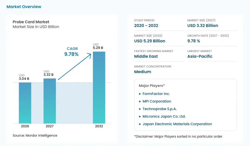
This report is segmented by Technology (MEMS, Vertical, and more), Application (Foundry and Logic, DRAM, and more), Type (Standard Probe Card and Advanced Probe Card), End User (Foundries, Integrated Device Manufacturers, and more), Wafer Size (300 mm, 200 mm, and more), and Geography (Asia-Pacific, North America, and more). The market forecasts are provided in terms of value (USD), based on availability.
Global Probe Card Market Trends and Insights
Rising Demand for Consumer Electronics and IoT Devices
Consumer-device production gives probe-card suppliers a demand channel within the broader technology spending cycle. The Consumer Technology Association (CTA) January 2026 forecast estimated US consumer technology retail revenue at USD 525 billion in 2025, up 3.9% from 2024. The estimate included hardware, software, and services. Xiaomi reported that its air-conditioner shipments exceeded 8.5 million units in 2025, a record high and up more than 24% year over year. For smart-home device programs using wafer-tested chips, additional unit production can increase the electrical screening required before assembly. Record appliance shipments at Xiaomi can therefore add demand for wafer-level chip screening where the additional devices require more wafer-tested semiconductors.
Miniaturization of Semiconductor Devices
Commercial miniaturization increases the importance of the electrical interface between a compact device and its test system. TSMC said N2, its 2-nanometer-class process, entered high-volume manufacturing in Q4 2025. On October 15, 2026, it reported that N2 was ramping successfully in multiple phases at Hsinchu and Kaohsiung in Taiwan. At the SWTest wafer-test conference in June 2026, Intel Foundry said improving yield in advanced system-on-chip packages with many dies requires core and micro-bump probing of compute dies, including at native pitches below 50 µm. This connects process scaling with a specific requirement to access increasingly compact electrical connections. A card that cannot probe micro-bumps at those pitches falls outside the requirement Intel Foundry described.
High Cost of Advanced Probe Card Development
Development costs constrain entry before a supplier can earn revenue from a qualified MEMS probe card. FormFactor's FY2025 annual report identifies high investment and development costs for MEMS probe cards, plus the time and cost of customer evaluation, as significant barriers to entry. The two-stage burden combines technology development with a separate customer-acceptance process. It can favor suppliers with designs already qualified for a buyer over entrants financing both stages. A technically viable new design can therefore remain commercially unavailable while its customer evaluation adds expense and time.
Other drivers and restraints analyzed in the detailed report include:
- Growth in Advanced Packaging and 3D IC Technologies
- Momentum in Foundry Expansion Incentive Programs
- Complexity of Testing at Sub-5 nm Nodes
For complete list of drivers and restraints, kindly check the Table Of Contents.
Segment Analysis
MEMS accounted for a 45.05% share of the probe card market size in 2026. In February 2026, Japan Electronic Materials Corporation resolved to build a factory in Amagasaki, Japan, to strengthen M-type MEMS probe-card production, with completion scheduled for August 2028. The plan paired stronger production capacity and efficiency with next-generation card development to respond to customer demand. Because the planned factory targets M-type MEMS cards specifically, Japan Electronic Materials is directing production efficiency and next-generation development into the technology with the largest share.
Vertical is the fastest-growing segment by technology, with a projected CAGR of 11.2% between 2027 and 2032. Cantilever cards face a distinct design trade-off, as a 2026 study of multilayer and 5-layer designs identified interference, unequal contact forces, and bond-pad scratch risks. Japan Electronic Materials Corporation reported that V-type cards accounted for 12% of its probe-card sales in April to June 2026. Its V-type family includes vertical probe series, a cantilever-structured series, and a vertical/cantilever hybrid, so this commercial base spans multiple contact architectures.
Foundry and logic represented a 47.62% probe card market share in 2026. FormFactor reported USD 121.8 million in Foundry & Logic revenue in Q2 2026, against USD 209.7 million for its Probe Cards segment. FormFactor's fiscal 2025 Foundry & Logic probe-card revenue was USD 369.9 million, down 3% from fiscal 2024. Its Q2 2025 Foundry & Logic revenue was USD 99.5 million, below the Q2 2026 reading. FormFactor's annual decline followed by a year-over-year quarterly increase shows that application leadership alone does not predict a supplier's revenue path.
Flash is the fastest-growing segment by application, with a projected CAGR of 11.5% between 2027 and 2032. On August 7, 2026, SK hynix announced plans for a NAND fab at Cheongju M17, citing surging enterprise SSD demand and targeting its first cleanroom opening for December 2028. The company linked that NAND demand to the full-scale expansion of AI services. With the first M17 cleanroom targeted for December 2028, card revenue from this fab is contingent on construction reaching production.
Complete Report Scope:
- By Technology
- MEMS
- Vertical
- Cantilever
- Specialty
- By Application
- DRAM
- Flash
- Foundry and Logic
- Parametric
- Other Applications
- By Type
- Standard Probe Card
- Advanced Probe Card
- By End User
- Foundries
- Integrated Device Manufacturers
- Outsourced Semiconductor Assembly and Test
- Research Institutes
- By Wafer Size
- 150 mm and Below
- 200 mm
- 300 mm
- 450 mm
- By Geography
- North America
- United States
- Canada
- Mexico
- South America
- Brazil
- Argentina
- Rest of South America
- Europe
- Germany
- France
- United Kingdom
- Italy
- Spain
- Russia
- Rest of Europe
- Asia-Pacific
- China
- Japan
- South Korea
- Taiwan
- India
- ASEAN
- Rest of Asia-Pacific
- Middle East
- Saudi Arabia
- United Arab Emirates
- Turkey
- Israel
- Rest of Middle East
- Africa
- South Africa
- Nigeria
- Kenya
- Egypt
- Rest of Africa
- North America
Geography Analysis
Asia-Pacific held an 84.28% share of the probe card market size in 2026, making it the largest geography. In Q2 2026, FormFactor reported companywide revenue shipped to Taiwan of USD 94.4 million and to South Korea of USD 73.4 million. South Korea represented 30.3% of its companywide ship-to revenue in fiscal 2025, when higher DRAM probe-card demand, including high-bandwidth memory (HBM) cards, contributed to increased revenue there. Taiwan was FormFactor's larger companywide destination in Q2 2026, but South Korea's fiscal 2025 growth had a specifically identified DRAM and HBM contribution, separating destination scale from memory-testing exposure within Asia-Pacific.
The Middle East is the fastest-growing geography, with a projected CAGR of 10.5% between 2027 and 2032. In its August 4, 2026 filing, Tower Semiconductor identified one operating 200 mm manufacturing facility in Israel. In April 2026, Tower reported implementing a USD 920 million multi-fab equipment investment to expand silicon germanium and silicon photonics capacity and develop next-generation capabilities. The aggregate plan covers Fabs 2, 3, 7, and 9, including Fab 2 in Migdal Haemek, Israel. Fab 2 in Migdal Haemek is the only one of those fabs in Israel, so prospective card business at that site is tied to its part of the manufacturing expansion.
North America gained upstream 300 mm wafer supply when GlobalWafers Co., Ltd. opened its silicon wafer plant in Sherman, Texas, on May 15, 2025, which serves device fabs rather than wafer-test lines. Europe's prospective wafer-test customer base gained a construction-stage project when Landesdirektion Sachsen issued European Semiconductor Manufacturing Company GmbH its first partial Dresden fab, utility, and ancillary-building permit on September 15, 2025. In South America, Brazil's National Institute for Space Research described its MIMEC laboratory in 2025 as national semiconductor research infrastructure for silicon micromechanics and MEMS. For Africa, World Economic Forum authors in 2025 identified assembly, testing, and packaging as a more accessible entry point than capital-intensive fabrication, making wafer-probe opportunities conditional on the testing operations developed. Upstream wafer supply, a permitted fab, research infrastructure, and a potential back-end entry route therefore offer distinct supplier conditions, with additional card demand dependent on their connection to device-level wafer testing.
- FormFactor Inc.
- Technoprobe S.p.A.
- Micronics Japan Co. Ltd.
- Japan Electronic Materials Corporation
- MPI Corporation
- Feinmetall GmbH
- Korea Instrument Co. Ltd.
- Wentworth Laboratories Inc.
- GGB Industries Inc.
- Protec MEMS Technology
- Nidec SV Probe Pte. Ltd.
- STAr Technologies Inc.
- Willtechnology Co. Ltd.
- TSE Co. Ltd.
- Chunghwa Precision Test Tech Co. Ltd.
- Protec MEMS Technology Inc.
- Synergie-Cad Probe
- T.I.P.S. Messtechnik GmbH
- Maxone Semiconductor (Suzhou) Co., Ltd.
- Shenzhen Fastprint Circuit Tech Co. Ltd.
Additional Benefits:
- The market estimate (ME) sheet in Excel format
- 3 months of analyst support
TABLE OF CONTENTS
1 INTRODUCTION
- 1.1 Study Assumptions and Market Definition
- 1.2 Scope of the Study
2 RESEARCH METHODOLOGY
3 EXECUTIVE SUMMARY
4 MARKET LANDSCAPE
- 4.1 Market Overview
- 4.2 Market Drivers
- 4.2.1 Rising Demand for Consumer Electronics and IoT Devices
- 4.2.2 Miniaturization of Semiconductor Devices
- 4.2.3 Growth in Advanced Packaging and 3D IC Technologies
- 4.2.4 Momentum in Foundry Expansion Incentive Programs
- 4.2.5 Shift Toward Less than 60 µm Vertical MEMS Probe Cards
- 4.2.6 Adoption of AI-Assisted Probe Card Alignment Systems
- 4.3 Market Restraints
- 4.3.1 High Cost of Advanced Probe Card Development
- 4.3.2 Complexity of Testing at Sub-5 nm Nodes
- 4.3.3 Cyclical Nature of Semiconductor Capital Expenditure
- 4.3.4 Limited Availability of Ultra-Low-Resistance Probe Materials
- 4.4 Industry Value Chain Analysis
- 4.5 Regulatory Landscape
- 4.6 Technological Outlook
- 4.7 Porter's Five Forces Analysis
- 4.7.1 Threat of New Entrants
- 4.7.2 Bargaining Power of Suppliers
- 4.7.3 Bargaining Power of Buyers
- 4.7.4 Threat of Substitutes
- 4.7.5 Competitive Rivalry
- 4.8 Pricing Trend Analysis
- 4.9 Analysis of RF Probe Cards
5 MARKET SIZE AND GROWTH FORECASTS (VALUE)
- 5.1 By Technology
- 5.1.1 MEMS
- 5.1.2 Vertical
- 5.1.3 Cantilever
- 5.1.4 Specialty
- 5.2 By Application
- 5.2.1 DRAM
- 5.2.2 Flash
- 5.2.3 Foundry and Logic
- 5.2.4 Parametric
- 5.2.5 Other Applications
- 5.3 By Type
- 5.3.1 Standard Probe Card
- 5.3.2 Advanced Probe Card
- 5.4 By End User
- 5.4.1 Foundries
- 5.4.2 Integrated Device Manufacturers
- 5.4.3 Outsourced Semiconductor Assembly and Test
- 5.4.4 Research Institutes
- 5.5 By Wafer Size
- 5.5.1 150 mm and Below
- 5.5.2 200 mm
- 5.5.3 300 mm
- 5.5.4 450 mm
- 5.6 By Geography
- 5.6.1 North America
- 5.6.1.1 United States
- 5.6.1.2 Canada
- 5.6.1.3 Mexico
- 5.6.2 South America
- 5.6.2.1 Brazil
- 5.6.2.2 Argentina
- 5.6.2.3 Rest of South America
- 5.6.3 Europe
- 5.6.3.1 Germany
- 5.6.3.2 France
- 5.6.3.3 United Kingdom
- 5.6.3.4 Italy
- 5.6.3.5 Spain
- 5.6.3.6 Russia
- 5.6.3.7 Rest of Europe
- 5.6.4 Asia-Pacific
- 5.6.4.1 China
- 5.6.4.2 Japan
- 5.6.4.3 South Korea
- 5.6.4.4 Taiwan
- 5.6.4.5 India
- 5.6.4.6 ASEAN
- 5.6.4.7 Rest of Asia-Pacific
- 5.6.5 Middle East
- 5.6.5.1 Saudi Arabia
- 5.6.5.2 United Arab Emirates
- 5.6.5.3 Turkey
- 5.6.5.4 Israel
- 5.6.5.5 Rest of Middle East
- 5.6.6 Africa
- 5.6.6.1 South Africa
- 5.6.6.2 Nigeria
- 5.6.6.3 Kenya
- 5.6.6.4 Egypt
- 5.6.6.5 Rest of Africa
- 5.6.1 North America
6 COMPETITIVE LANDSCAPE
- 6.1 Market Concentration
- 6.2 Strategic Moves
- 6.3 Market Share Analysis
- 6.4 Company Profiles (includes Global level Overview, Market level overview, Core Segments, Financials as available, Strategic Information, Market Rank/Share for key companies, Products and Services, and Recent Developments)
- 6.4.1 FormFactor Inc.
- 6.4.2 Technoprobe S.p.A.
- 6.4.3 Micronics Japan Co. Ltd.
- 6.4.4 Japan Electronic Materials Corporation
- 6.4.5 MPI Corporation
- 6.4.6 Feinmetall GmbH
- 6.4.7 Korea Instrument Co. Ltd.
- 6.4.8 Wentworth Laboratories Inc.
- 6.4.9 GGB Industries Inc.
- 6.4.10 Protec MEMS Technology
- 6.4.11 Nidec SV Probe Pte. Ltd.
- 6.4.12 STAr Technologies Inc.
- 6.4.13 Willtechnology Co. Ltd.
- 6.4.14 TSE Co. Ltd.
- 6.4.15 Chunghwa Precision Test Tech Co. Ltd.
- 6.4.16 Protec MEMS Technology Inc.
- 6.4.17 Synergie-Cad Probe
- 6.4.18 T.I.P.S. Messtechnik GmbH
- 6.4.19 Maxone Semiconductor (Suzhou) Co., Ltd.
- 6.4.20 Shenzhen Fastprint Circuit Tech Co. Ltd.
7 MARKET OPPORTUNITIES AND FUTURE OUTLOOK
- 7.1 White-Space and Unmet-Need Assessment

