
PUBLISHER: Mordor Intelligence | PRODUCT CODE: 1690752

PUBLISHER: Mordor Intelligence | PRODUCT CODE: 1690752
Semiconductor Lithography Equipment - Market Share Analysis, Industry Trends & Statistics, Growth Forecasts (2025 - 2030)
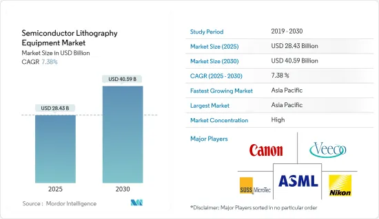
The Semiconductor Lithography Equipment Market size is estimated at USD 28.43 billion in 2025, and is expected to reach USD 40.59 billion by 2030, at a CAGR of 7.38% during the forecast period (2025-2030).
Key Highlights
- The semiconductor lithography equipment market is expected to grow with the growing manufacturing of semiconductor devices that are widely used in nearly all sectors including consumer electronics, automotive, and many others. Smart device adoption is increasing and is expected to grow as 5G connections and adoption spread over the globe. As per GSMA, 5G mobile broadband connections are expected to reach 1,100 million by 2025, with the 5G rollout expected to cover 34 percent of the world's population by 2025.
- More than 50 percent of the semiconductor FAB (fabrication) cost is due to equipment and tools. One piece of equipment that drives the semiconductor fabrication process forward is lithography. There are several aspects of semiconductor fabrication that has driven by lithography equipment. Yield and defect are two such examples from the technical point of view. It is the primary reason why semiconductor fabrication focuses a lot on which type of lithography technology to deploy.
- With the rising complexity in semiconductor products, the types of defects are also getting complex. However, lithography equipment is supposed to handle the complex process. With semiconductor manufacturers focusing on next-gen advanced technology nodes, the importance of error-free lithography equipment is significantly increasing further.
- Moreover, manufacturing businesses are are lately growing at a signficant rate with the advent of 5G and emergence of IoT connected devices, which is anticipated to facilitate the connection required for various Industry 4.0 applications, such as wireless control. This is especially essential for mobile tools, machines, and robots that can aid market growth during the forecast period.
- Several industry players are focusing on offering new lithography systems to serve a wide range of applications. For instance, in March 2022, Nikon Corporation announced to launch new Gen 8 plate FPD lithography system to support the production of various high-definition panels for value-added premium displays, such as high-end monitors, large TVs, and smart devices.
- The semiconductor industry is considered as one of the most complex industries, not only owing to the presence of more than 500 processing steps involved in the manufacturing and inspection and various products but also due to the harsh environment it goes through, e.g., the volatile electronic market and the unpredictable demand. Therefore, depending on the intricacy of the manufacturing process, there are about 1,400 process steps in the complete manufacturing and inspection of semiconductor wafers alone. Such a complex process poses a notable hurdle to the market's growth.
Semiconductor Lithography Equipment Market Trends
Deep Ultraviolet Lithography (DUV) to Hold Major Market Share
- Deep UV lithography (DUV) is an optical projection lithography technique where the pattern on the mask is projected to the wafer surface through a 4X or 5X optical system. The wavelengths used for this type of lithography are 248 nm or 193 nm. This lithography is a high-speed lithographic technology ideal for large-area masters of discrete components that are not bigger than 22 mm x 22 mm, the typical wafer-level exposure field size of a DUV tool.
- The DUV lithography type is one of the leading lithography technologies of the next generation. The technology is cost-effective and has increased resolving power. The adoption of DUV lithography is driven primarily by the miniaturization trend. Lithography is used for printing complex patterns that characterize integrated circuits (ICs) on semiconductor wafers.
- Using DUV lithography, lightweight electronic chips with lower power demands are easy to achieve. The platform features enhanced power resolution and is cost-effective. These structures together form an IC, which is known as a chip. The semiconductor industry's search for even more efficient microchips means chipmakers have to study more structures onto a chip, making the chip faster and more efficient while also reducing production costs. This is expected to boost the market's growth over the forecast period.
- According to ASML, a transition to EUV may only boost demand for DUV. Chip manufacturers deploy EUV in the early stages of chip fabrication to apply the minor structures: transistors, smallest vias (the contacts that connect the source, gate, and drain to the complex interconnect layers), and possibly the connecting layer.
- According to WSTS, Semiconductor sales in Europe reached 4.42 billion USD in January 2024, a slight decrease from the 4.48 billion USD reported in January 2023. Global semiconductor sales hit 47.63 billion U.S. dollars in January 2024 when considering the overall market.
- Such developments by the major vendors, along with the initiatives taken by the government to boost their semiconductor production, are expected to drive market growth over the forecast period.
United States to Witness Significant Share
- The United States boasts robust semiconductor R&D capabilities, significant investments catering to the expansion of semiconductor manufacturing capabilities, and rapid adoption of advanced technologies.
- Further, the United States is witnessing an increasing demand for semiconductors. For instance, in September 2021, according to the world semiconductor trade statistics (WSTS), semiconductor industry sales increased significantly to USD 527 billion in 2021, an upward revision from the 2020 forecast for 2021 due mainly to the strong demand growth in the overall market 2020. In 2022, WSTS forecasted global sales totaled to USD 573 billion.
- Additionally, in April 2022, according to Semiconductor Equipment and Materials International, North America's spending on semiconductor equipment reached USD 7.61 billion in 2021 compared to 2020, which was USD 6.53 billion.
- Also, the semiconductor industry association stated that the US semiconductor industry is a leader in chip design. The United States fabless firms account for roughly 60 percent of all global fabless firm sales, and some of the largest IDMs, which make their arrangement, are also US firms.
- According to the state of the US semiconductors industry, the connected devices that run on semiconductor chips (i.e., the Internet of Things (IoT)) registered USD 22.6 billion in 2019 and are expected to reach USD 75 billion by 2025. Semiconductors are also fundamental to innovations, such as 3D printing, machine learning, and artificial intelligence (AI) that enhance healthcare, reduce building costs, strengthen food supply, and enable advancements in science. The region's robust semiconductor demand is likely to boost the adoption of semiconductor lithography equipment during the forecast period.
- Additionally, in September 2022, the Biden administration announced that it would invest USD 50 billion in building up the domestic semiconductor industry to counter dependency on China, as the US produces zero and consumes 25 percent of the world's leading-edge chips vital for its national security. President Joe Biden signed a USD 280 billion CHIPS bill in August 2022 to boost domestic high-tech manufacturing, part of his administration's push to boost US competitiveness over China. Such robust investments in the semiconductor sector in the region would offer lucrative opportunities for the growth of the studied market.
Semiconductor Lithography Equipment Industry Overview
The market is concentrated due to a few vendors such as ASML, Veeco, and Nikon occupying the majority market share. The key equipment for semiconductor manufacturing is basically monopolized by American and Japanese companies. With growing consolidation and technological advancement, and geopolitical scenarios, the studied market is witnessing fluctuation. In addition, with increasing vertical integration, the intensity of competition in the studied market is expected to continue to rise, considering their ability to invest, which results from their revenues.
- September 2022 - Canon Inc. launched the "Lithography Plus1" solution platform for semiconductor lithography systems. Canon's more than 50 years of experience in semiconductor lithography system support and the company's vast wealth of data are incorporated into the system to maximize support efficiency and propose and implement optimized system processes.
- June 2022 - Samsung and ASML have agreed to collaborate on developing High-NA (high numerical aperture) EUV Lithography equipment, which will be available next year. Compared to older EUV Lithography equipment, the next-generation High-NA EUV Lithography equipment can engrave finer circuits.
Additional Benefits:
- The market estimate (ME) sheet in Excel format
- 3 months of analyst support
TABLE OF CONTENTS
1 INTRODUCTION
- 1.1 Study Assumptions and Market Definition
- 1.2 Scope of the Study
2 RESEARCH METHODOLOGY
3 EXECUTIVE SUMMARY
4 MARKET INSIGHTS
- 4.1 Market Overview
- 4.2 Industry Attractiveness - Porter's Five Forces Analysis
- 4.2.1 Bargaining Power of Suppliers
- 4.2.2 Bargaining Power of Buyers
- 4.2.3 Threat of New Entrants
- 4.2.4 Threat of Substitute Products
- 4.2.5 Intensity of Competitive Rivalry
- 4.3 Semiconductor Lithography Equipment Technology Roadmap
- 4.4 The impact of macroeconomic trends on the Market
5 MARKET DYNAMICS
- 5.1 Market Drivers
- 5.1.1 Increasing Demand for Miniaturization and Extra Functionality by Electric Vehicles and Advanced Mobile Devices
- 5.1.2 Growing Innovation by Specialist Equipment Vendors offering Brand New Lithography Tools
- 5.2 Market Restraints
- 5.2.1 Challenges Regarding Complexity of Pattern in Manufacturing Process
6 MARKET SEGMENTATION
- 6.1 Type
- 6.1.1 Deep Ultraviolet Lithography (DUV)
- 6.1.2 Extreme Ultraviolet Lithography (EUV)
- 6.2 Application
- 6.2.1 Advanced Packaging
- 6.2.2 MEMS Devices
- 6.2.3 LED Devices
- 6.3 Geography
- 6.3.1 North America
- 6.3.2 Europe
- 6.3.3 Asia
- 6.3.4 Australia and New Zealand
- 6.3.5 Latin America
- 6.3.6 Middle East and Africa
7 COMPETITIVE LANDSCAPE
- 7.1 Company Profiles
- 7.1.1 Canon Inc.
- 7.1.2 Nikon Corporation
- 7.1.3 ASML Holding NV
- 7.1.4 Veeco Instruments Inc.
- 7.1.5 SUSS MicroTec SE
- 7.1.6 Shanghai Micro Electronics Equipment (Group) Co. Ltd
- 7.1.7 EV Group (EVG)
- 7.1.8 JEOL Ltd
- 7.1.9 Onto Innovation (Rudolph Technologies Inc.)
- 7.1.10 Neutronix Quintel Inc. (NXQ)
- 7.2 Vendor Market Share Analysis
8 INVESTMENT ANALYSIS
9 FUTURE OF THE MARKET

