
PUBLISHER: Aviation & Defense Market Reports (A&D) | PRODUCT CODE: 2072233

PUBLISHER: Aviation & Defense Market Reports (A&D) | PRODUCT CODE: 2072233
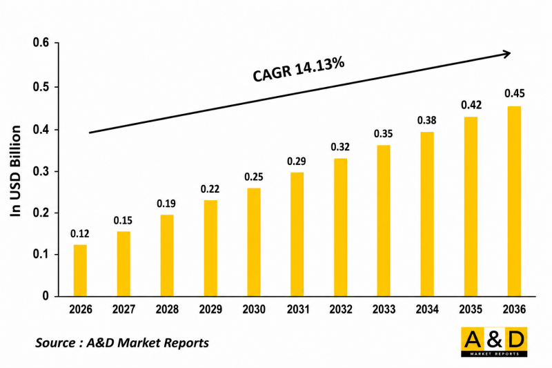
Global Boundary Scan Test Systems 2026-2036
Global Boundary Scan Test Systems Market
The Global Boundary Scan Test Systems is estimated at USD 0.12 billion in 2026, projected to grow to USD 0.45 billion by 2036 at a Compound Annual Growth Rate (CAGR) of 14.13% over the forecast period 2026-2036.
1. Introduction
Boundary scan test systems are essential electronic testing solutions used to verify the integrity and functionality of printed circuit boards and semiconductor devices. These systems enable manufacturers to identify defects, connectivity issues, and assembly errors without requiring direct physical access to components. In industries where reliability and performance are critical, boundary scan technologies play a significant role in ensuring product quality and reducing maintenance costs. The growing complexity of electronic systems in aerospace, defense, automotive, and telecommunications sectors has increased the importance of advanced testing methods. Boundary scan solutions support efficient fault detection during manufacturing and throughout the product lifecycle. They also contribute to reducing development time and enhancing product reliability. As electronic architectures become increasingly sophisticated, manufacturers are adopting automated testing platforms capable of supporting miniaturized components and complex integrated circuits, making boundary scan test systems an indispensable element of modern electronics production and quality assurance processes.
2. Technology Impact in Global Boundary Scan Test Systems Market
Technological advancements are transforming boundary scan test systems by improving test coverage, automation, and diagnostic capabilities. Modern solutions integrate software-driven analysis tools and support complex multilayer circuit designs, enabling faster identification of faults. Artificial intelligence and machine learning technologies are enhancing predictive diagnostics and reducing manual intervention during testing procedures. Cloud-based test management platforms provide remote access and centralized monitoring, improving operational efficiency across distributed manufacturing facilities. Integration with automated production environments allows seamless data exchange and real-time quality control. Advanced interfaces and high-speed communication protocols support next-generation electronic architectures with increased component density. Miniaturization trends in semiconductor devices have also encouraged the development of highly accurate testing methodologies. These innovations are improving production yields, reducing costs, and enabling manufacturers to maintain high reliability standards across increasingly complex electronic systems.
3. Key Drivers in Global Boundary Scan Test Systems Market
The increasing complexity of electronic assemblies is a major factor driving demand for boundary scan test systems. Manufacturers require efficient testing solutions to ensure product reliability while minimizing production delays. Rising adoption of advanced semiconductor devices and multilayer circuit boards has created the need for sophisticated fault detection technologies. The aerospace and defense sectors place significant emphasis on reliability and compliance with stringent quality standards, further encouraging adoption of automated testing solutions. Growing demand for connected devices and communication systems has increased the volume of complex electronics requiring comprehensive inspection. Manufacturers are also focusing on reducing operational costs and enhancing production efficiency through automation. In addition, the trend toward digital manufacturing and smart factories has accelerated integration between testing systems and production processes. Continuous advancements in electronic design and increasing emphasis on reducing product failures are expected to sustain demand for boundary scan technologies across various industries.
4. Regional Trends in Global Boundary Scan Test Systems Market
North America remains a prominent market due to strong aerospace, defense, and semiconductor industries that require highly reliable testing solutions. Europe emphasizes advanced manufacturing standards and quality assurance, supporting widespread adoption of boundary scan technologies. The Asia-Pacific region is experiencing significant growth driven by expanding electronics manufacturing capabilities and increasing investments in semiconductor production. Countries with strong consumer electronics and telecommunications industries are strengthening demand for automated testing systems. Rising industrialization and growing electronics exports are also supporting market expansion across emerging economies. In the Middle East, increasing investments in defense electronics and industrial automation are encouraging adoption of advanced inspection technologies. Latin America is gradually expanding its manufacturing base, creating opportunities for modern testing solutions. Across regions, the transition toward digital manufacturing and greater focus on quality assurance continue to support the deployment of boundary scan test systems.
5. Key Global Boundary Scan Test Systems Market Program
Manufacturers and technology providers are introducing advanced programs aimed at improving testing efficiency and supporting increasingly complex electronic systems. These initiatives focus on enhancing software capabilities, expanding compatibility with emerging semiconductor architectures, and improving automation across production lines. Industry collaborations are promoting standardization and interoperability among testing platforms, ensuring broader adoption across different applications. Research and development programs emphasize predictive diagnostics, artificial intelligence integration, and cloud-based data management solutions. Semiconductor manufacturers are also investing in next-generation inspection methodologies to address miniaturization challenges. Training and certification programs are being introduced to help engineers maximize the effectiveness of boundary scan technologies. These efforts are strengthening product quality, reducing manufacturing costs, and supporting the growing demand for reliable electronic systems in aerospace, defense, telecommunications, and industrial applications.
Table of Contents
Global Aerospace and Defense Boundary Scan Test Systems Market Report Definition
Global Aerospace and Defense Boundary Scan Test Systems Market Segmentation
- By Region
- By Component
- By Technology
- By Application
Global Aerospace and Defense Boundary Scan Test Systems Market Analysis for next 10 Years
The 10-year Global Aerospace and Defense Boundary Scan Test Systems market analysis would give a detailed overview of Global Aerospace and Defense Boundary Scan Test Systems market growth, changing dynamics, technology adoption overviews and the overall market attractiveness is covered in this chapter.
Market Technologies of Global Aerospace and Defense Boundary Scan Test Systems Market
This segment covers the top 10 technologies that is expected to impact this market and the possible implications these technologies would have on the overall market.
Global Global Aerospace and Defense Boundary Scan Test Systems Market Forecast
The 10-year Global Aerospace and Defense Boundary Scan Test Systems market forecast of this market is covered in detailed across the segments which are mentioned above.
Regional Global Aerospace and Defense Boundary Scan Test Systems Market Trends & Forecast
The regional Global Aerospace and Defense Boundary Scan Test Systems market trends, drivers, restraints and Challenges of this market, the Political, Economic, Social and Technology aspects are covered in this segment. The market forecast and scenario analysis across regions are also covered in detailed in this segment. The last part of the regional analysis includes profiling of the key companies, supplier landscape and company benchmarking. The current market size is estimated based on the normal scenario.
- North America
- Drivers, Restraints and Challenges
- PEST
- Market Forecast & Scenario Analysis
- Key Companies
- Supplier Tier Landscape
- Company Benchmarking
- Europe
- Middle East
- APAC
- South America
Country Analysis of Global Aerospace and Defense Boundary Scan Test Systems Market
This chapter deals with the key defense programs in this market, it also covers the latest news and patents which have been filed in this market. Country level 10 year market forecast and scenario analysis are also covered in this chapter.
- US
- Defense Programs
- Latest News
- Patents
- Current levels of technology maturation in this market
- Market Forecast & Scenario Analysis
- Canada
- Italy
- France
- Germany
- Netherlands
- Belgium
- Spain
- Sweden
- Greece
- Australia
- South Africa
- India
- China
- Russia
- South Korea
- Japan
- Malaysia
- Singapore
- Brazil
Opportunity Matrix for Global Aerospace and Defense Boundary Scan Test Systems Market
The opportunity matrix helps the readers understand the high opportunity segments in this market.
Expert Opinions on Global Aerospace and Defense Boundary Scan Test Systems Market Report
Hear from our experts their opinion of the possible analysis for this market.
Conclusions
About Aviation and Defense Market Reports
List of Tables
- Table 1: 10 Year Market Outlook, 2026-2036
- Table 2: Drivers, Impact Analysis, North America
- Table 3: Restraints, Impact Analysis, North America
- Table 4: Challenges, Impact Analysis, North America
- Table 5: Drivers, Impact Analysis, Europe
- Table 6: Restraints, Impact Analysis, Europe
- Table 7: Challenges, Impact Analysis, Europe
- Table 8: Drivers, Impact Analysis, Middle East
- Table 9: Restraints, Impact Analysis, Middle East
- Table 10: Challenges, Impact Analysis, Middle East
- Table 11: Drivers, Impact Analysis, Apac
- Table 12: Restraints, Impact Analysis, Apac
- Table 13: Challenges, Impact Analysis, Apac
- Table 14: Drivers, Impact Analysis, South America
- Table 15: Restraints, Impact Analysis, South America
- Table 16: Challenges, Impact Analysis, South America
- Table 17: Scenario Analysis, Scenario 1, By Region, 2026-2036
- Table 18: Scenario Analysis, Scenario 1, By Technology 2026-2036
- Table 19: Scenario Analysis, Scenario 1, By Component, 2026-2036
- Table 20: Scenario Analysis, Scenario 2, By Region, 2026-2036
- Table 21: Scenario Analysis, Scenario 2, By Technology 2026-2036
- Table 22: Scenario Analysis, Scenario 2, By Component, 2026-2036
List of Figures
- Figure 1: Global Defense Boundary Scan Test Systems Market Forecast, 2026-2036
- Figure 2: Global Defense Boundary Scan Test Systems Market Forecast, By Region, 2026-2036
- Figure 3: Global Defense Boundary Scan Test Systems Market Forecast, By Technology 2026-2036
- Figure 4: Global Defense Boundary Scan Test Systems Market Forecast, By Component, 2026-2036
- Figure 5: North America, Defense Boundary Scan Test Systems Market, Market Forecast, 2026-2036
- Figure 6: Europe, Defense Boundary Scan Test Systems Market, Market Forecast, 2026-2036
- Figure 7: Middle East, Defense Boundary Scan Test Systems Market, Market Forecast, 2026-2036
- Figure 8: Apac, Defense Boundary Scan Test Systems Market, Market Forecast, 2026-2036
- Figure 9: South America, Defense Boundary Scan Test Systems Market, Market Forecast, 2026-2036
- Figure 10: United States, Defense Boundary Scan Test Systems Market, Region Maturation, 2026-2036
- Figure 11: United States, Defense Boundary Scan Test Systems Market, Market Forecast, 2026-2036
- Figure 12: Canada, Defense Boundary Scan Test Systems Market, Region Maturation, 2026-2036
- Figure 13: Canada, Defense Boundary Scan Test Systems Market, Market Forecast, 2026-2036
- Figure 14: Italy, Defense Boundary Scan Test Systems Market, Region Maturation, 2026-2036
- Figure 15: Italy, Defense Boundary Scan Test Systems Market, Market Forecast, 2026-2036
- Figure 16: France, Defense Boundary Scan Test Systems Market, Region Maturation, 2026-2036
- Figure 17: France, Defense Boundary Scan Test Systems Market, Market Forecast, 2026-2036
- Figure 18: Germany, Defense Boundary Scan Test Systems Market, Region Maturation, 2026-2036
- Figure 19: Germany, Defense Boundary Scan Test Systems Market, Market Forecast, 2026-2036
- Figure 20: Netherlands, Defense Boundary Scan Test Systems Market, Region Maturation, 2026-2036
- Figure 21: Netherlands, Defense Boundary Scan Test Systems Market, Market Forecast, 2026-2036
- Figure 22: Belgium, Defense Boundary Scan Test Systems Market, Region Maturation, 2026-2036
- Figure 23: Belgium, Defense Boundary Scan Test Systems Market, Market Forecast, 2026-2036
- Figure 24: Spain, Defense Boundary Scan Test Systems Market, Region Maturation, 2026-2036
- Figure 25: Spain, Defense Boundary Scan Test Systems Market, Market Forecast, 2026-2036
- Figure 26: Sweden, Defense Boundary Scan Test Systems Market, Region Maturation, 2026-2036
- Figure 27: Sweden, Defense Boundary Scan Test Systems Market, Market Forecast, 2026-2036
- Figure 28: Brazil, Defense Boundary Scan Test Systems Market, Region Maturation, 2026-2036
- Figure 29: Brazil, Defense Boundary Scan Test Systems Market, Market Forecast, 2026-2036
- Figure 30: Australia, Defense Boundary Scan Test Systems Market, Region Maturation, 2026-2036
- Figure 31: Australia, Defense Boundary Scan Test Systems Market, Market Forecast, 2026-2036
- Figure 32: India, Defense Boundary Scan Test Systems Market, Region Maturation, 2026-2036
- Figure 33: India, Defense Boundary Scan Test Systems Market, Market Forecast, 2026-2036
- Figure 34: China, Defense Boundary Scan Test Systems Market, Region Maturation, 2026-2036
- Figure 35: China, Defense Boundary Scan Test Systems Market, Market Forecast, 2026-2036
- Figure 36: Saudi Arabia, Defense Boundary Scan Test Systems Market, Region Maturation, 2026-2036
- Figure 37: Saudi Arabia, Defense Boundary Scan Test Systems Market, Market Forecast, 2026-2036
- Figure 38: South Korea, Defense Boundary Scan Test Systems Market, Region Maturation, 2026-2036
- Figure 39: South Korea, Defense Boundary Scan Test Systems Market, Market Forecast, 2026-2036
- Figure 40: Japan, Defense Boundary Scan Test Systems Market, Region Maturation, 2026-2036
- Figure 41: Japan, Defense Boundary Scan Test Systems Market, Market Forecast, 2026-2036
- Figure 42: Malaysia, Defense Boundary Scan Test Systems Market, Region Maturation, 2026-2036
- Figure 43: Malaysia, Defense Boundary Scan Test Systems Market, Market Forecast, 2026-2036
- Figure 44: Singapore, Defense Boundary Scan Test Systems Market, Region Maturation, 2026-2036
- Figure 45: Singapore, Defense Boundary Scan Test Systems Market, Market Forecast, 2026-2036
- Figure 46: United Kingdom, Defense Boundary Scan Test Systems Market, Region Maturation, 2026-2036
- Figure 47: United Kingdom, Defense Boundary Scan Test Systems Market, Market Forecast, 2026-2036
- Figure 48: Opportunity Analysis, Defense Boundary Scan Test Systems Market, By Region (Cumulative Market), 2026-2036
- Figure 49: Opportunity Analysis, Defense Boundary Scan Test Systems Market, By Region (Cagr), 2026-2036
- Figure 50: Opportunity Analysis, Defense Boundary Scan Test Systems Market, By Technology Cumulative Market), 2026-2036
- Figure 51: Opportunity Analysis, Defense Boundary Scan Test Systems Market, By Technology (Cagr), 2026-2036
- Figure 52: Opportunity Analysis, Defense Boundary Scan Test Systems Market, By Component(Cumulative Market), 2026-2036
- Figure 53: Opportunity Analysis, Defense Boundary Scan Test Systems Market, By Component (Cagr), 2026-2036
- Figure 54: Scenario Analysis, Defense Boundary Scan Test Systems Market, Cumulative Market, 2026-2036
- Figure 55: Scenario Analysis, Defense Boundary Scan Test Systems Market, Global Market, 2026-2036
- Figure 56: Scenario 1, Defense Boundary Scan Test Systems Market, Total Market, 2026-2036
- Figure 57: Scenario 1, Defense Boundary Scan Test Systems Market, By Region, 2026-2036
- Figure 58: Scenario 1, Defense Boundary Scan Test Systems Market, By Technology 2026-2036
- Figure 59: Scenario 1, Defense Boundary Scan Test Systems Market, By Component, 2026-2036
- Figure 60: Scenario 2, Defense Boundary Scan Test Systems Market, Total Market, 2026-2036
- Figure 61: Scenario 2, Defense Boundary Scan Test Systems Market, By Region, 2026-2036
- Figure 62: Scenario 2, Defense Boundary Scan Test Systems Market, By Technology 2026-2036
- Figure 63: Scenario 2, Defense Boundary Scan Test Systems Market, By Component, 2026-2036
- Figure 64: Company Benchmark, Defense Boundary Scan Test Systems Market, 2026-2036

