
PUBLISHER: Global Market Insights Inc. | PRODUCT CODE: 2038293

PUBLISHER: Global Market Insights Inc. | PRODUCT CODE: 2038293
Semiconductor Inspection Systems Market Opportunity, Growth Drivers, Industry Trend Analysis, and Forecast 2026 - 2035
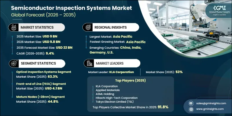
The Global Semiconductor Inspection Systems Market was valued at USD 9 billion in 2025 and is estimated to grow at a CAGR of 9.4% to reach USD 22 billion by 2035.
Increasing intricacy in semiconductor architectures and the shift toward highly integrated device structures are significantly elevating the need for advanced inspection capabilities. The rising demand for high-performance computing and data-driven applications is accelerating production volumes, placing greater emphasis on quality control and defect minimization. Manufacturers are increasingly prioritizing early-stage defect identification and yield enhancement strategies to maintain efficiency across fabrication processes. In addition, continuous investment in semiconductor manufacturing infrastructure across multiple regions is reinforcing the demand for high-precision inspection tools. As fabrication processes evolve, the integration of advanced inspection technologies is becoming essential to ensure consistency, improve throughput, and support next-generation semiconductor innovation.
| Market Scope | |
|---|---|
| Start Year | 2025 |
| Forecast Year | 2026-2035 |
| Start Value | $9 Billion |
| Forecast Value | $22 Billion |
| CAGR | 9.4% |
The semiconductor inspection systems market is shaped by the increasing sophistication of device manufacturing and the transition toward advanced process technologies. As semiconductor structures become more compact and complex, maintaining precision and minimizing variability across production stages has become critical. This has led to a stronger focus on comprehensive inspection processes that support early fault detection and stable production cycles. The expansion of semiconductor manufacturing facilities across global markets is also contributing to the widespread deployment of inspection equipment throughout the production lifecycle, from initial development to large-scale manufacturing.
The e-beam inspection systems segment is expected to grow at a CAGR of 11.6% during 2026-2035, driven by the rising need for highly detailed defect detection. These systems are increasingly utilized for their ability to identify extremely small imperfections and provide precise analytical insights that enhance process optimization. Their relevance continues to grow as semiconductor manufacturing requires greater accuracy and finer resolution to maintain product quality and performance standards.
The front-end-of-line segment reached USD 4.1 billion in 2025. This segment remains critical due to the need for continuous inspection during early manufacturing stages, where maintaining structural accuracy and consistency is essential. Frequent monitoring during these processes helps reduce defect rates and supports higher production yields, sustaining demand for inspection technologies.
North America Semiconductor Inspection Systems Market accounted for 28.5% share in 2025. Growth in the region is being supported by increased investment to strengthen domestic semiconductor manufacturing capabilities. The expansion of fabrication facilities and ongoing advancements in production technologies are driving demand for inspection solutions that ensure operational efficiency and product quality. The region continues to see strong adoption of advanced inspection systems as manufacturers scale up production to meet growing technological demands.
Key companies operating in the Global Semiconductor Inspection Systems Market include Applied Materials, KLA Corporation, ASML Holding, Hitachi High-Tech Corporation, Tokyo Electron Limited (TEL), Onto Innovation Inc., Lasertec Corporation, Camtek Ltd., SCREEN Semiconductor Solutions, Nova Ltd., Advantest Corporation, ZEISS Group (Carl Zeiss SMT), Toray Engineering Co., Ltd., Muetec Inc., and RSIC Scientific Instrument Co., Ltd. Companies in the Semiconductor Inspection Systems Market are enhancing their competitive position through continuous innovation and strategic expansion initiatives. They are investing in research and development to introduce advanced inspection technologies capable of addressing increasing manufacturing complexity. Many players are integrating artificial intelligence and data analytics into their systems to improve defect detection accuracy and process efficiency. Strategic partnerships and collaborations are helping companies expand their technological capabilities and global reach. Additionally, firms are strengthening their supply chains and establishing new production facilities to meet rising demand. A strong focus on customer-centric solutions, along with long-term service and support offerings, is also enabling companies to build lasting relationships and maintain a competitive edge.
Table of Contents
Chapter 1 Methodology and Scope
- 1.1 Market scope and definition
- 1.2 Research design
- 1.2.1 Research approach
- 1.2.2 Data collection methods
- 1.3 Data mining sources
- 1.3.1 Global
- 1.3.2 Regional/Country
- 1.4 Base estimates and calculations
- 1.4.1 Base year calculation
- 1.4.2 Key trends for market estimation
- 1.5 Primary research and validation
- 1.5.1 Primary sources
- 1.6 Forecast model
- 1.7 Research assumptions and limitations
Chapter 2 Executive Summary
- 2.1 Industry 360° synopsis, 2022 - 2035
- 2.2 Key market trends
- 2.2.1 Technology type trends
- 2.2.2 System type trends
- 2.2.3 Process stage trends
- 2.2.4 Node type trends
- 2.2.5 Deployment type trends
- 2.2.6 End-user trends
- 2.2.7 Regional trends
- 2.3 TAM Analysis, 2026-2035
- 2.4 CXO perspectives: Strategic imperatives
Chapter 3 Industry Insights
- 3.1 Industry ecosystem analysis
- 3.1.1 Supplier Landscape
- 3.1.2 Profit Margin
- 3.1.3 Cost structure
- 3.1.4 Value addition at each stage
- 3.1.5 Factor affecting the value chain
- 3.1.6 Disruptions
- 3.2 Industry impact forces
- 3.2.1 Growth drivers
- 3.2.1.1 Increasing device complexity at advanced and next-generation nodes
- 3.2.1.2 Rapid adoption of advanced packaging and heterogeneous integration
- 3.2.1.3 Rising semiconductor demand driven by AI, HPC, and data-centric applications
- 3.2.1.4 Increasing process control intensity to improve yield and time-to-market
- 3.2.1.5 Expansion of global fab capacity and localization of semiconductor manufacturing
- 3.2.2 Industry pitfalls and challenges
- 3.2.2.1 High capital cost and complexity of advanced inspection systems
- 3.2.2.2 Data overload and integration challenges in inspection workflows
- 3.2.3 Market opportunities
- 3.2.3.1 Expansion of advanced packaging and chiplet-based architectures
- 3.2.3.2 Rising adoption of AI-enabled inspection and analytics platforms
- 3.2.1 Growth drivers
- 3.3 Growth potential analysis
- 3.4 Regulatory landscape
- 3.4.1 North America
- 3.4.2 Europe
- 3.4.3 Asia Pacific
- 3.4.4 Latin America
- 3.4.5 Middle East & Africa
- 3.5 Porter's analysis
- 3.6 PESTEL analysis
- 3.7 Technology and Innovation landscape
- 3.7.1 Current technological trends
- 3.7.2 Emerging technologies
- 3.8 Price trends
- 3.8.1 By region
- 3.8.2 By product
- 3.9 Pricing Strategies
- 3.10 Emerging Business Models
- 3.11 Compliance Requirements
- 3.12 Patent and IP analysis
Chapter 4 Competitive Landscape, 2025
- 4.1 Introduction
- 4.2 Company market share analysis
- 4.2.1 By region
- 4.2.1.1 North America
- 4.2.1.2 Europe
- 4.2.1.3 Asia Pacific
- 4.2.1.4 Latin America
- 4.2.1.5 Middle East & Africa
- 4.2.2 Market concentration analysis
- 4.2.1 By region
- 4.3 Competitive benchmarking of key players
- 4.3.1 Financial performance comparison
- 4.3.1.1 Revenue
- 4.3.1.2 Profit margin
- 4.3.1.3 R&D
- 4.3.2 Product portfolio comparison
- 4.3.2.1 Product range breadth
- 4.3.2.2 Technology
- 4.3.2.3 Innovation
- 4.3.3 Geographic presence comparison
- 4.3.3.1 Global footprint analysis
- 4.3.3.2 Service network coverage
- 4.3.3.3 Market penetration by region
- 4.3.4 Competitive positioning matrix
- 4.3.4.1 Leaders
- 4.3.4.2 Challengers
- 4.3.4.3 Followers
- 4.3.4.4 Niche players
- 4.3.5 Strategic outlook matrix
- 4.3.1 Financial performance comparison
- 4.4 Key developments
- 4.4.1 Mergers and acquisitions
- 4.4.2 Partnerships and collaborations
- 4.4.3 Technological advancements
- 4.4.4 Expansion and investment strategies
- 4.4.5 Digital transformation initiatives
- 4.5 Emerging/ startup competitors landscape
Chapter 5 Market Estimates and Forecast, By Technology Type, 2022 - 2035 (USD Million)
- 5.1 Key trends
- 5.2 Optical inspection systems
- 5.3 E-beam inspection systems
Chapter 6 Market Estimates and Forecast, By System Type, 2022 - 2035 (USD Million)
- 6.1 Key trends
- 6.2 Patterned wafer inspection systems
- 6.3 Unpatterned wafer inspection systems
- 6.4 Mask/reticle inspection systems
- 6.5 Packaging & substrate inspection systems
Chapter 7 Market Estimates and Forecast, By Process Stage, 2022 - 2035 (USD Million)
- 7.1 Key trends
- 7.2 Front-end of line (FEOL)
- 7.3 Back-end of line (BEOL)
- 7.4 Advanced packaging
Chapter 8 Market Estimates and Forecast, By Node Type, 2022 - 2035 (USD Million)
- 8.1 Key trends
- 8.2 Advanced nodes (≤7nm)
- 8.3 Intermediate nodes (8-28nm)
- 8.4 Mature nodes (>28nm)
Chapter 9 Market Estimates and Forecast, By Deployment Type, 2022 - 2035 (USD Million)
- 9.1 Key trends
- 9.2 In-line inspection systems
- 9.3 Standalone inspection systems
- 9.4 Closed-loop / integrated process control systems
Chapter 10 Market Estimates and Forecast, By End-User, 2022 - 2035 (USD Million)
- 10.1 Key trends
- 10.2 Foundries
- 10.3 IDMs - logic
- 10.4 IDMs - memory
- 10.5 OSATs
Chapter 11 Market Estimates and Forecast, By Region, 2022 - 2035 (USD Million)
- 11.1 Key trends
- 11.2 North America
- 11.2.1 U.S.
- 11.2.2 Canada
- 11.3 Europe
- 11.3.1 Germany
- 11.3.2 UK
- 11.3.3 France
- 11.3.4 Spain
- 11.3.5 Italy
- 11.3.6 Russia
- 11.4 Asia Pacific
- 11.4.1 China
- 11.4.2 India
- 11.4.3 Japan
- 11.4.4 Australia
- 11.4.5 South Korea
- 11.5 Latin America
- 11.5.1 Brazil
- 11.5.2 Mexico
- 11.5.3 Argentina
- 11.6 Middle East and Africa
- 11.6.1 South Africa
- 11.6.2 Saudi Arabia
- 11.6.3 UAE
Chapter 12 Company Profiles
- 12.1 Global Key Players
- 12.1.1 KLA Corporation
- 12.1.2 Applied Materials
- 12.1.3 ASML Holding
- 12.1.4 Hitachi High-Tech Corporation
- 12.1.5 Tokyo Electron Limited (TEL)
- 12.2 Regional key players
- 12.2.1 North America
- 12.2.1.1 Onto Innovation Inc.
- 12.2.1.2 RSIC Scientific Instrument Co., Ltd.
- 12.2.2 Asia Pacific
- 12.2.2.1 Lasertec Corporation
- 12.2.2.2 SCREEN Semiconductor Solutions
- 12.2.2.3 Advantest Corporation
- 12.2.2.4 Toray Engineering Co., Ltd.
- 12.2.2.5 Muetec Inc.
- 12.2.3 Europe
- 12.2.3.1 ZEISS Group (Carl Zeiss SMT)
- 12.2.3.2 Camtek Ltd.
- 12.2.3.3 Nova Ltd.
- 12.2.1 North America
- 12.3 Niche Players/Disruptors
- 12.3.1 Muetec Inc.
- 12.3.2 RSIC Scientific Instrument Co., Ltd.

