
PUBLISHER: Global Market Insights Inc. | PRODUCT CODE: 1721493

PUBLISHER: Global Market Insights Inc. | PRODUCT CODE: 1721493
3D Stacking Market Opportunity, Growth Drivers, Industry Trend Analysis, and Forecast 2025 - 2034
The Global 3D Stacking Market was valued at USD 1.8 billion in 2024 and is expected to grow at a CAGR of 21.1% to reach USD 11.8 billion by 2034. This remarkable growth is largely attributed to the rising demand for consumer electronics, high-performance computing systems, and advanced semiconductor technologies. As data-intensive applications such as artificial intelligence (AI), machine learning, and the Internet of Things (IoT) continue to scale, the need for faster data processing, enhanced efficiency, and improved power management becomes more critical than ever. 3D stacking technology is increasingly seen as the future of semiconductor innovation, enabling device manufacturers to meet these evolving needs by integrating multiple functional layers-such as logic, memory, and interconnects-within a compact footprint. As the electronics industry pushes toward miniaturization without compromising performance, 3D stacking provides an ideal pathway to achieve higher throughput, lower latency, and superior thermal management. From smartphones and wearables to data center processors and autonomous vehicles, the scope of applications for this technology is rapidly expanding. The adoption of chiplet-based designs and heterogeneous integration further drives this market's momentum, offering the flexibility to customize solutions for specific use cases across industries.
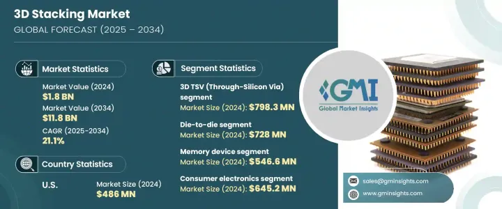
3D stacking technology is classified based on interconnection methods, including 3D hybrid bonding, 3D Through-Silicon Via (TSV), and monolithic 3D integration. Among these, the 3D TSV segment generated USD 798.3 million in 2024. This segment is experiencing robust growth due to rising demand for high-speed, low-latency memory interfaces that support the performance requirements of data centers, HPC platforms, and autonomous systems. The rollout of 5G networks and the proliferation of smart devices are also intensifying the need for energy-efficient and compact chip architectures that can manage vast volumes of real-time data processing.
| Market Scope | |
|---|---|
| Start Year | 2024 |
| Forecast Year | 2025-2034 |
| Start Value | $1.8 Billion |
| Forecast Value | $11.8 Billion |
| CAGR | 21.1% |
The market is further segmented by interconnect technology, including die-to-wafer, wafer-to-wafer, die-to-die, chip-to-chip, and chip-to-wafer techniques. The die-to-die segment was valued at USD 728 million in 2024. This method is especially vital for multi-chip modules and chipset-based architectures that require seamless communication between dies. It plays a key role in advancing AI accelerators, cloud infrastructure, and HPC processors, offering greater design flexibility, enhanced energy savings, and improved scalability.
United States 3D Stacking Market generated USD 486 million in 2024. The region is witnessing substantial growth owing to increased investments in AI applications, advanced data center operations, and HPC infrastructure. US-based semiconductor firms are channeling resources into developing chiplet architectures and TSV-based designs to push the boundaries of performance, energy efficiency, and scalability in next-gen computing.
Key players in the Global 3D Stacking Market include AMD, ASE Technology Holding, Amkor Technology, Broadcom, IBM, Intel, Graphcore, JCET Group, Marvell Technology, Micron Technology, Kioxia, NVIDIA, OmniVision Technologies, SK Hynix, Sony Semiconductor Solutions, Samsung Electronics, SPIL, Western Digital, and Xilinx. These companies are accelerating innovations in chip stacking and interconnect methodologies to address the growing demand from AI, data center, and high-performance computing markets. Through focused R&D and strategic investments, they aim to deliver future-ready semiconductor solutions that combine power efficiency, superior performance, and architectural flexibility.
Table of Contents
Chapter 1 Methodology and Scope
- 1.1 Market scope and definitions
- 1.2 Research design
- 1.2.1 Research approach
- 1.2.2 Data collection methods
- 1.3 Base estimates and calculations
- 1.3.1 Base year calculation
- 1.3.2 Key trends for market estimation
- 1.4 Forecast model
- 1.5 Primary research and validation
- 1.5.1 Primary sources
- 1.5.2 Data mining sources
Chapter 2 Executive Summary
- 2.1 Industry 3600 synopsis
Chapter 3 Industry Insights
- 3.1 Industry ecosystem analysis
- 3.2 Industry impact forces
- 3.2.1 Growth drivers
- 3.2.1.1 Rising demand for high-performance computing (HPC)
- 3.2.1.2 Expanding applications in AI and edge computing
- 3.2.1.3 Growth in consumer electronics
- 3.2.1.4 Increase in automotive and IoT applications
- 3.2.1.5 Growth in memory and storage demand
- 3.2.2 Industry pitfalls and challenges
- 3.2.2.1 High manufacturing costs and complexity
- 3.2.2.2 Thermal and power management issues
- 3.2.1 Growth drivers
- 3.3 Growth potential analysis
- 3.4 Regulatory landscape
- 3.5 Technology landscape
- 3.6 Future market trends
- 3.7 Gap analysis
- 3.8 Porter’s analysis
- 3.9 PESTEL analysis
Chapter 4 Competitive Landscape, 2024
- 4.1 Introduction
- 4.2 Company market share analysis
- 4.3 Competitive analysis of major market players
- 4.4 Competitive positioning matrix
- 4.5 Strategy dashboard
Chapter 5 Market Estimates and Forecast, By Method, 2021 – 2034 (USD Million)
- 5.1 Key trends
- 5.2 Die-to-Die
- 5.3 Die-to-Wafer
- 5.4 Wafer-to-Wafer
- 5.5 Chip-to-Chip
- 5.6 Chip-to-Wafer
Chapter 6 Market Estimates and Forecast, By Interconnecting Technology, 2021 – 2034 (USD Million)
- 6.1 Key trends
- 6.2 3D hybrid bonding
- 6.3 3D TSV (Through-Silicon Via)
- 6.4 Monolithic 3D Integration
Chapter 7 Market Estimates and Forecast, By Device Type, 2021 – 2034 (USD Million)
- 7.1 Key trends
- 7.2 Logic ICs
- 7.3 Imaging & Optoelectronics
- 7.4 Memory devices
- 7.5 MEMS/Sensors
- 7.6 LEDs
- 7.7 Others (RF, photonics, analog & mixed signals, and power devices)
Chapter 8 Market Estimates and Forecast, By End Use Industry, 2021 – 2034 (USD Million)
- 8.1 Key trends
- 8.2 Consumer electronics
- 8.3 Manufacturing
- 8.4 Communications (Telecommunication, Data Centers & HPC)
- 8.5 Automotive
- 8.6 Medical Devices/Healthcare
- 8.7 Others (Military & Defence, Aviation)
Chapter 9 Market Estimates and Forecast, By Region, 2021 – 2034 (USD Million)
- 9.1 Key trends
- 9.2 North America
- 9.2.1 U.S.
- 9.2.2 Canada
- 9.3 Europe
- 9.3.1 Germany
- 9.3.2 UK
- 9.3.3 France
- 9.3.4 Spain
- 9.3.5 Italy
- 9.3.6 Netherlands
- 9.4 Asia Pacific
- 9.4.1 China
- 9.4.2 India
- 9.4.3 Japan
- 9.4.4 Australia
- 9.4.5 South Korea
- 9.5 Latin America
- 9.5.1 Brazil
- 9.5.2 Mexico
- 9.5.3 Argentina
- 9.6 Middle East and Africa
- 9.6.1 Saudi Arabia
- 9.6.2 South Africa
- 9.6.3 UAE
Chapter 10 Company Profiles
- 10.1 AMD
- 10.2 Amkor Technology
- 10.3 ASE Technology Holding
- 10.4 Broadcom
- 10.5 Graphcore
- 10.6 IBM
- 10.7 Intel
- 10.8 JCET Group
- 10.9 Kioxia
- 10.10 Marvell Technology
- 10.11 Micron Technology
- 10.12 NVIDIA
- 10.13 OmniVision Technologies
- 10.14 Samsung Electronics
- 10.15 SK Hynix
- 10.16 Sony Semiconductor Solutions
- 10.17 SPIL
- 10.18 TSMC
- 10.19 Western Digital
- 10.20 Xilinx

