
PUBLISHER: Global Market Insights Inc. | PRODUCT CODE: 1892717

PUBLISHER: Global Market Insights Inc. | PRODUCT CODE: 1892717
Atomic Layer Etching (ALE) Equipment Market Opportunity, Growth Drivers, Industry Trend Analysis, and Forecast 2025 - 2034
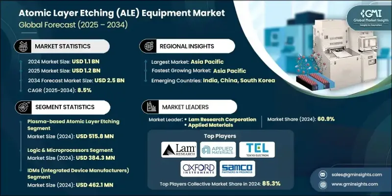
The Global Atomic Layer Etching Equipment Market was valued at USD 1.1 billion in 2024 and is estimated to grow at a CAGR of 8.5% to reach USD 2.5 billion by 2034.
Growth is fueled by rising demand for compact, high-performance semiconductor components, rapid advancements in quantum technologies, and the push for energy-efficient electronics. Companies are also responding to the adoption of new materials and the ongoing trend toward greater device miniaturization, which requires etching capabilities with atomic-level precision. As next-generation chips continue to increase in complexity, the industry is seeing a strong shift toward advanced tools capable of supporting sophisticated architecture. The momentum generated by quantum research is also boosting the need for highly accurate etching techniques that improve the fabrication of extremely sensitive components.
| Market Scope | |
|---|---|
| Start Year | 2024 |
| Forecast Year | 2025-2034 |
| Start Value | $1.1 billion |
| Forecast Value | $2.5 billion |
| CAGR | 8.5% |
The plasma-based atomic layer etching segment held USD 515.8 million in 2024. Continued expansion in microelectronics is encouraging suppliers to enhance plasma ALE portfolios that deliver greater precision, improved etch selectivity, and tighter material control to meet rising production requirements across advanced manufacturing environments.
The advanced packaging devices segment will grow at 11.4% CAGR between 2025 and 2034. Its growth is linked to increasing performance demands, the spread of 5G connectivity, and the need to integrate more functionality without redesigning core devices. Companies are prioritizing innovations in thermal efficiency, miniaturization, and high-density interconnect technologies to support evolving packaging requirements in modern electronic systems.
United States Atomic Layer Etching Equipment Market generated USD 200.2 million in 2024. This expansion stems from federal funding for semiconductor capacity, a surge in AI and IoT development, progress in advanced manufacturing nodes, and elevated demand from defense-oriented applications. Companies operating in the region are leveraging investment incentives, strengthening next-generation process capabilities, and addressing the sophisticated needs of aerospace and defense customers.
Key players in the Atomic Layer Etching Equipment Market include Lam Research Corporation, CORIAL, NAURA, Mattson Technology, Inc., Oxford Instruments, Samco Inc., Tokyo Electron, Applied Materials, Hitachi High-Tech Corporation, and Nano Vacuum Pty Ltd. Companies competing in the Atomic Layer Etching Equipment Market are adopting strategic measures to reinforce their global positions. Many are investing heavily in R&D programs to enhance precision, boost throughput, and improve compatibility with emerging materials. Businesses are also expanding collaboration with semiconductor manufacturers to co-develop etch solutions aligned with next-generation device architectures. Several players are strengthening production capacity and broadening product portfolios to address varied fabrication needs. Firms are increasing their presence in high-growth regions by forming local partnerships and establishing technical support centers.
Table of Contents
Chapter 1 Methodology and scope
- 1.1 Market scope and definition
- 1.2 Research design
- 1.2.1 Research approach
- 1.2.2 Data collection methods
- 1.3 Data mining sources
- 1.3.1 Global
- 1.3.2 Regional/Country
- 1.4 Base estimates and calculations
- 1.4.1 Base year calculation
- 1.4.2 Key trends for market estimation
- 1.5 Primary research and validation
- 1.5.1 Primary sources
- 1.6 Forecast model
- 1.7 Research assumptions and limitations
Chapter 2 Executive summary
- 2.1 Industry 3600 synopsis
- 2.2 Key market trends
- 2.2.1 Technology trend
- 2.2.2 Application trends
- 2.2.3 Wafer size trends
- 2.2.4 End use industry trends
- 2.2.5 Regional trends
- 2.3 TAM Analysis, 2025-2034 (USD Million)
- 2.4 CXO perspectives: Strategic imperatives
- 2.4.1 Executive decision points
- 2.4.2 critical success factors
- 2.5 Future outlook and strategic recommendations
Chapter 3 Industry insights
- 3.1 Industry ecosystem analysis
- 3.1.1 Supplier landscape
- 3.1.2 Profit margin
- 3.1.3 Cost structure
- 3.1.4 Value addition at each stage
- 3.1.5 Factor affecting the value chain
- 3.1.6 Disruptions
- 3.2 Industry ecosystem analysis
- 3.3 Industry impact forces
- 3.3.1 Growth drivers
- 3.3.1.1 Increasing Demand for Smaller and More Powerful Semiconductor Devices
- 3.3.1.2 Advancements in Quantum Computing
- 3.3.1.3 Growing Demand for High-Performance and Energy-Efficient Electronics
- 3.3.1.4 Emergence of New Materials for Advanced Electronics
- 3.3.1.5 Rising Demand for Miniaturized and Complex Integrated Circuits
- 3.3.2 Pitfalls and challenges
- 3.3.2.1 High Cost of ALE Equipment
- 3.3.2.2 Complexity in Integration with Existing Manufacturing Processes
- 3.3.3 Market opportunities
- 3.3.3.1 Rising Demand for Advanced Semiconductor Technologies
- 3.3.3.2 Growth of Emerging Applications in IoT and AI
- 3.3.1 Growth drivers
- 3.4 Growth potential analysis
- 3.5 Regulatory landscape
- 3.5.1 North America
- 3.5.2 Europe
- 3.5.3 Asia Pacific
- 3.5.4 Latin America
- 3.5.5 Middle East & Africa
- 3.6 Porter's analysis
- 3.7 PESTEL analysis
- 3.8 Technology and Innovation landscape
- 3.8.1 Current technological trends
- 3.8.2 Emerging technologies
- 3.9 Price trends
- 3.9.1 By region
- 3.9.2 By product
- 3.10 Pricing Strategies
- 3.11 Emerging Business Models
- 3.12 Compliance Requirements
- 3.13 Sustainability Measures
- 3.14 Consumer Sentiment Analysis
- 3.15 Patent and IP analysis
- 3.16 Geopolitical and trade dynamics
Chapter 4 Competitive landscape, 2024
- 4.1 Introduction
- 4.2 Company market share analysis
- 4.2.1 By region
- 4.2.1.1 North America
- 4.2.1.2 Europe
- 4.2.1.3 Asia Pacific
- 4.2.1.4 Latin America
- 4.2.1.5 Middle East & Africa
- 4.2.2 Market concentration analysis
- 4.2.1 By region
- 4.3 Competitive benchmarking of key players
- 4.3.1 Financial performance comparison
- 4.3.1.1 Revenue
- 4.3.1.2 Profit margin
- 4.3.1.3 R&D
- 4.3.2 Product portfolio comparison
- 4.3.2.1 Product range breadth
- 4.3.2.2 Technology
- 4.3.2.3 Innovation
- 4.3.3 Geographic presence comparison
- 4.3.3.1 Global footprint analysis
- 4.3.3.2 Service network coverage
- 4.3.3.3 Market penetration by region
- 4.3.4 Competitive positioning matrix
- 4.3.4.1 Leaders
- 4.3.4.2 Challengers
- 4.3.4.3 Followers
- 4.3.4.4 Niche players
- 4.3.5 Strategic outlook matrix
- 4.3.1 Financial performance comparison
- 4.4 Key developments, 2021-2024
- 4.4.1 Mergers and acquisitions
- 4.4.2 Partnerships and collaborations
- 4.4.3 Technological advancements
- 4.4.4 Expansion and investment strategies
- 4.4.5 Sustainability initiatives
- 4.4.6 Digital transformation initiatives
- 4.5 Emerging/ startup competitors landscape
Chapter 5 Market estimates and forecast, by Technology, 2021 - 2034 (USD Million & Units)
- 5.1 Key trends
- 5.2 Plasma-based atomic layer etching
- 5.3 Ion beam atomic layer etching
- 5.4 Thermal atomic layer etching
- 5.5 Hybrid atomic layer etching
- 5.6 Others
Chapter 6 Market estimates and forecast, By Application, 2021 - 2034 (USD Million & Units)
- 6.1 Key trends
- 6.2 Logic & microprocessors
- 6.3 Memory devices
- 6.4 Power & RF devices
- 6.5 Advanced packaging
- 6.6 Optoelectronics & photonics
- 6.7 MEMS & sensors
- 6.8 Others
Chapter 7 Market estimates and forecast, By Wafer Size, 2021 - 2034 (USD Million & Units)
- 7.1 Key trends
- 7.2 200 mm
- 7.3 300 mm
- 7.4 450 mm
Chapter 8 Market estimates and forecast, By End Use, 2021 - 2034 (USD Million & Units)
- 8.1 Key trends
- 8.2 IDMs (integrated device manufacturers)
- 8.3 Foundries
- 8.4 Memory manufacturers
- 8.5 OSATs / packaging houses
- 8.6 Others
Chapter 9 Market estimates and forecast, By Region, 2021 - 2034 (USD Million & Units)
- 9.1 Key trends
- 9.2 North America
- 9.2.1 U.S.
- 9.2.2 Canada
- 9.3 Europe
- 9.3.1 Germany
- 9.3.2 UK
- 9.3.3 France
- 9.3.4 Spain
- 9.3.5 Italy
- 9.3.6 Netherlands
- 9.4 Asia Pacific
- 9.4.1 China
- 9.4.2 India
- 9.4.3 Japan
- 9.4.4 Australia
- 9.4.5 South Korea
- 9.5 Latin America
- 9.5.1 Brazil
- 9.5.2 Mexico
- 9.5.3 Argentina
- 9.6 Middle East and Africa
- 9.6.1 Saudi Arabia
- 9.6.2 South Africa
- 9.6.3 UAE
Chapter 10 Company profiles
- 10.1 Global Key Players
- 10.1.1 Lam Research Corporation
- 10.1.2 Applied Materials
- 10.1.3 Tokyo Electron
- 10.1.4 Hitachi High Tech Corporation
- 10.2 Regional Key Players
- 10.2.1 North America
- 10.2.1.1 Mattson Technology, Inc.
- 10.2.1.2 Plasma-Therm
- 10.2.2 Europe
- 10.2.2.1 Oxford Instruments
- 10.2.3 Asia-Pacific
- 10.2.3.1 Samco Inc.
- 10.2.3.2 Nano Vacuum Pty Ltd
- 10.2.1 North America
- 10.3 Disruptors / Niche Players
- 10.3.1 CORIAL

