
PUBLISHER: Global Market Insights Inc. | PRODUCT CODE: 1959280

PUBLISHER: Global Market Insights Inc. | PRODUCT CODE: 1959280
Advanced Semiconductor Packaging Market Opportunity, Growth Drivers, Industry Trend Analysis, and Forecast 2026 - 2035
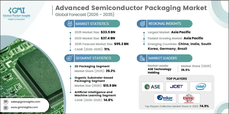
The Global Advanced Semiconductor Packaging Market was valued at USD 33.5 billion in 2025 and is estimated to grow at a CAGR of 11% to reach USD 95.3 billion by 2035.
Market expansion is fueled by the increasing transition toward chiplet-based processor architectures and the widespread deployment of next-generation wireless infrastructure. These trends are accelerating demand for high-density radio frequency integration and system-in-package configurations that support compact, high-performance electronics. At the same time, escalating fabrication costs and yield constraints at leading-edge process nodes are shifting industry focus toward advanced packaging as a critical driver of performance gains and cost efficiency. The growing adoption of AI accelerators that require high-bandwidth memory integration is further strengthening demand, as these configurations enable extremely high data throughput essential for advanced computing workloads. In addition, expansion of hyperscale data centers and high-performance computing platforms is driving the implementation of 2.5D and 3D integrated circuit architectures. These packaging innovations enable heterogeneous integration, improved interconnect density, and enhanced power efficiency, reinforcing their strategic importance in next-generation semiconductor design.
| Market Scope | |
|---|---|
| Start Year | 2025 |
| Forecast Year | 2026-2035 |
| Start Value | $33.5 Billion |
| Forecast Value | $95.3 Billion |
| CAGR | 11% |
In 2025, the 2D packaging segment accounted for 29.2% share, maintaining the largest share. Its continued dominance is supported by strong utilization across mature logic nodes, analog components, power management devices, and mixed-signal integrated circuits. This packaging format remains highly attractive for large-scale production due to its cost stability, manufacturing reliability, and optimized yield performance. Key end-use industries, including consumer electronics, automotive systems, and industrial automation, continue to depend on 2D packaging because it aligns seamlessly with established fabrication processes and resilient supply networks. Its scalability and proven reliability ensure consistent demand across high-volume production environments.
The organic substrate-based packaging segment reached USD 13.9 billion in 2025. Growth in this category is driven by widespread deployment in flip-chip assemblies and advanced laminate package designs used in processors, connectivity components, and automotive electronics. Organic substrates provide an optimal combination of electrical performance, mechanical flexibility, and cost efficiency, making them well-suited for applications requiring high input/output density. Established production ecosystems and continuous material innovation further reinforce segment growth. Demand remains strong across consumer devices, communications infrastructure, and industrial systems, where performance consistency and manufacturability at scale are essential.
North America Advanced Semiconductor Packaging Market held a 22.8% share in 2025. The region is experiencing accelerated development driven by rising demand for AI-enabled processors and advanced data center chips. A robust ecosystem of integrated device manufacturers and outsourced semiconductor assembly and test providers supports rapid adoption of advanced packaging technologies. Increasing implementation of 2.5D and 3D integration strategies is helping regional players overcome performance, bandwidth, and power limitations associated with conventional planar architectures. Continued investment in semiconductor research, domestic manufacturing capabilities, and advanced computing infrastructure is further strengthening North America's competitive position in the global market.
Key companies operating in the Global Advanced Semiconductor Packaging Market include Taiwan Semiconductor Manufacturing Company (TSMC), Samsung Electronics, Intel Corporation, Amkor Technology, Inc., ASE Technology Holding, JCET Group Co., Ltd., Powertech Technology Inc. (PTI), GlobalFoundries Inc., Micron Technology, Inc., SK hynix, Texas Instruments, Tongfu Microelectronics Co., Ltd., Huatian Technology Co., Ltd., ChipMOS Technologies Inc., HANA Micron Inc., China Wafer Level CSP Co., Ltd. (CWLP), and UTAC Holdings Ltd. Companies in the Advanced Semiconductor Packaging Market are reinforcing their market position through strategic investments in research and development focused on high-density interconnect technologies and advanced substrate materials. Many players are expanding manufacturing capacity to meet rising demand from AI, high-performance computing, and automotive electronics sectors. Collaborative partnerships with foundries, memory manufacturers, and system designers are enabling co-optimization of chip architecture and packaging solutions. Firms are also prioritizing vertical integration to improve supply chain resilience and reduce production bottlenecks.
Table of Contents
Chapter 1 Methodology and Scope
- 1.1 Market scope and definition
- 1.2 Research design
- 1.2.1 Research approach
- 1.2.2 Data collection methods
- 1.3 Data mining sources
- 1.3.1 Global
- 1.3.2 Regional/Country
- 1.4 Base estimates and calculations
- 1.4.1 Base year calculation
- 1.4.2 Key trends for market estimation
- 1.5 Primary research and validation
- 1.5.1 Primary sources
- 1.6 Forecast model
- 1.7 Research assumptions and limitations
Chapter 2 Executive Summary
- 2.1 Industry 360° synopsis, 2022 - 2035
- 2.2 Key market trends
- 2.2.1 Packaging architecture trends
- 2.2.2 Packaging material trends
- 2.2.3 Application trends
- 2.2.4 Regional trends
- 2.3 TAM Analysis, 2026-2035
- 2.4 CXO perspectives: Strategic imperatives
- 2.4.1 Executive decision points
- 2.4.2 critical success factors
- 2.5 Future outlook and strategic recommendations
Chapter 3 Industry Insights
- 3.1 Industry ecosystem analysis
- 3.1.1 Supplier Landscape
- 3.1.2 Profit Margin
- 3.1.3 Cost structure
- 3.1.4 Value addition at each stage
- 3.1.5 Factor affecting the value chain
- 3.1.6 Disruptions
- 3.2 Industry impact forces
- 3.2.1 Growth drivers
- 3.2.1.1 AI accelerators demanding high-bandwidth memory integration
- 3.2.1.2 HPC and data centers adopting 2.5D and 3D ICs
- 3.2.1.3 Chiplet architectures replacing monolithic SoC designs
- 3.2.1.4 5G base stations requiring high-density RF packaging
- 3.2.1.5 Advanced nodes cost pushing value toward packaging innovation
- 3.2.2 Industry pitfalls and challenges
- 3.2.2.1 High capital expenditure for advanced packaging fabs
- 3.2.2.2 Thermal management complexity in high-power packaged devices
- 3.2.3 Market opportunities
- 3.2.3.1 Foundry-OSAT partnerships for advanced packaging capacity expansion
- 3.2.3.2 Co-packaged optics enabling next-generation data center interconnects
- 3.2.1 Growth drivers
- 3.3 Growth potential analysis
- 3.4 Regulatory landscape
- 3.4.1 North America
- 3.4.2 Europe
- 3.4.3 Asia Pacific
- 3.4.4 Latin America
- 3.4.5 Middle East & Africa
- 3.5 Porter's analysis
- 3.6 PESTEL analysis
- 3.7 Technology and Innovation landscape
- 3.7.1 Current technological trends
- 3.7.2 Emerging technologies
- 3.8 Price trends
- 3.8.1 By region
- 3.8.2 By product
- 3.9 Pricing Strategies
- 3.10 Emerging Business Models
- 3.11 Compliance Requirements
- 3.12 Patent and IP analysis
- 3.13 Geopolitical and trade dynamics
Chapter 4 Competitive Landscape, 2025
- 4.1 Introduction
- 4.2 Company market share analysis
- 4.2.1 By region
- 4.2.1.1 North America
- 4.2.1.2 Europe
- 4.2.1.3 Asia Pacific
- 4.2.1.4 Latin America
- 4.2.1.5 Middle East & Africa
- 4.2.2 Market concentration analysis
- 4.2.1 By region
- 4.3 Competitive benchmarking of key players
- 4.3.1 Financial performance comparison
- 4.3.1.1 Revenue
- 4.3.1.2 Profit margin
- 4.3.1.3 R&D
- 4.3.2 Product portfolio comparison
- 4.3.2.1 Product range breadth
- 4.3.2.2 Technology
- 4.3.2.3 Innovation
- 4.3.3 Geographic presence comparison
- 4.3.3.1 Global footprint analysis
- 4.3.3.2 Service network coverage
- 4.3.3.3 Market penetration by region
- 4.3.4 Competitive positioning matrix
- 4.3.4.1 Leaders
- 4.3.4.2 Challengers
- 4.3.4.3 Followers
- 4.3.4.4 Niche players
- 4.3.5 Strategic outlook matrix
- 4.3.1 Financial performance comparison
- 4.4 Key developments
- 4.4.1 Mergers and acquisitions
- 4.4.2 Partnerships and collaborations
- 4.4.3 Technological advancements
- 4.4.4 Expansion and investment strategies
- 4.4.5 Digital transformation initiatives
- 4.5 Emerging/ startup competitors landscape
Chapter 5 Market Estimates and Forecast, By Packaging Architecture, 2022 - 2035 (USD Million)
- 5.1 Key trends
- 5.2 2D Packaging (single-die, single-plane)
- 5.3 2.5D Packaging (multi-die, interposer-based, single vertical plane)
- 5.4 3D Packaging (Vertical Die Stacking)
- 5.4.1 TSV-based 3D packaging
- 5.4.2 Hybrid bonding-based 3D packaging
- 5.5 Wafer-level packaging (WLP)
- 5.5.1 Fan-in wafer-level packaging (FI-WLP)
- 5.5.2 Fan-out wafer-level packaging (FO-WLP)
- 5.6 Hybrid/multi-architecture packaging
Chapter 6 Market Estimates and Forecast, By Packaging Material, 2022 - 2035 (USD Million)
- 6.1 Key trends
- 6.2 Organic substrate-based packaging
- 6.3 Silicon interposer-based packaging
- 6.4 RDL-based (reconstituted wafer) packaging
- 6.5 3D stack-dominant packaging (die-to-die material platform)
- 6.6 Glass interposer-based packaging
Chapter 7 Market Estimates and Forecast, By Application, 2022 - 2035 (USD Million)
- 7.1 Key trends
- 7.2 Artificial intelligence and machine learning
- 7.3 High-performance computing (HPC) and data center
- 7.4 Mobile and communications
- 7.5 Automotive
- 7.6 Consumer electronics
- 7.7 Industrial, aerospace and defense
Chapter 8 Market Estimates and Forecast, By Region, 2022 - 2035 (USD Million)
- 8.1 Key trends
- 8.2 North America
- 8.2.1 U.S.
- 8.2.2 Canada
- 8.3 Europe
- 8.3.1 Germany
- 8.3.2 UK
- 8.3.3 France
- 8.3.4 Spain
- 8.3.5 Italy
- 8.3.6 Russia
- 8.4 Asia Pacific
- 8.4.1 China
- 8.4.2 India
- 8.4.3 Japan
- 8.4.4 Australia
- 8.4.5 South Korea
- 8.5 Latin America
- 8.5.1 Brazil
- 8.5.2 Mexico
- 8.5.3 Argentina
- 8.6 Middle East and Africa
- 8.6.1 South Africa
- 8.6.2 Saudi Arabia
- 8.6.3 UAE
Chapter 9 Company Profiles
- 9.1 Global Key Players
- 9.1.1 ASE Technology Holding
- 9.1.2 Amkor Technology, Inc.
- 9.1.3 Taiwan Semiconductor Manufacturing Company (TSMC)
- 9.1.4 Samsung Electronics
- 9.1.5 Intel Corporation
- 9.2 Regional key players
- 9.2.1 North America
- 9.2.1.1 GlobalFoundries Inc.
- 9.2.1.2 Texas Instruments
- 9.2.1.3 Micron Technology, Inc.
- 9.2.2 Asia Pacific
- 9.2.2.1 JCET Group Co., Ltd.
- 9.2.2.2 Powertech Technology Inc. (PTI)
- 9.2.2.3 Huatian Technology Co., Ltd.
- 9.2.2.4 Tongfu Microelectronics Co., Ltd.
- 9.2.2.5 ChipMOS Technologies Inc.
- 9.2.2.6 UTAC Holdings Ltd.
- 9.2.2.7 HANA Micron Inc.
- 9.2.2.8 SK hynix
- 9.2.1 North America
- 9.3 Niche Players/Disruptors
- 9.3.1 China Wafer Level CSP Co., Ltd. (CWLP)

