
PUBLISHER: Global Market Insights Inc. | PRODUCT CODE: 2038295

PUBLISHER: Global Market Insights Inc. | PRODUCT CODE: 2038295
EUV Mask Inspection Market Opportunity, Growth Drivers, Industry Trend Analysis, and Forecast 2026 - 2035
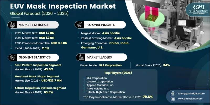
The Global EUV Mask Inspection Market was valued at USD 1.2 billion in 2025 and is estimated to grow at a CAGR of 11.1% to reach USD 3.3 billion by 2035.
Growth in the EUV mask inspection industry is being fueled by the expanding adoption of EUV lithography in advanced chip fabrication, which requires extremely precise defect detection capabilities. As mask complexity continues to increase, the risk of defects also rises, driving demand for more advanced inspection technologies. Semiconductor manufacturers are prioritizing high-yield production and pushing for defect-free processes, which is accelerating investment in next-generation inspection systems. At the same time, the expansion of EUV mask manufacturing infrastructure and ongoing technological advancements are reinforcing market growth, positioning the EUV mask inspection market as a critical component in next-generation semiconductor production.
| Market Scope | |
|---|---|
| Start Year | 2025 |
| Forecast Year | 2026-2035 |
| Start Value | $1.2 Billion |
| Forecast Value | $3.3 Billion |
| CAGR | 11.1% |
The EUV mask inspection market is further supported by the growing reliance on EUV lithography for advanced semiconductor production. As manufacturing processes become more sensitive, the need for highly accurate inspection solutions is increasing significantly. The push toward zero-defect production is encouraging the adoption of advanced inspection systems capable of detecting even the smallest irregularities. This shift is strengthening demand for high-performance inspection technologies that ensure reliability and yield optimization across semiconductor manufacturing processes.
The requalification and in-line inspection segment is expected to grow at a CAGR of 12% during 2026-2035. This growth is driven by the increasing use of EUV masks in high-volume manufacturing environments, where continuous monitoring is essential to maintain performance and quality. The need for frequent inspection cycles is accelerating the adoption of automated and high-resolution inspection systems, making this segment one of the fastest-growing in the EUV mask inspection market.
The merchant mask shops segment reached USD 523.7 million in 2025. This segment holds a strong position due to its extensive involvement in mask production and servicing for multiple semiconductor manufacturers. The need to ensure consistent quality and defect-free output across various production requirements is driving continuous demand for advanced inspection solutions within this segment.
North America EUV Mask Inspection Market accounted for 28.5% share in 2025, supported by significant investments in semiconductor manufacturing and advanced fabrication technologies. The region is witnessing increasing deployment of EUV-related infrastructure, which is driving demand for high-precision inspection systems. Strong support from government initiatives aimed at strengthening domestic semiconductor capabilities is further contributing to market growth across North America.
Key companies operating in the EUV Mask Inspection Market include ASML Holding N.V., KLA Corporation, Applied Materials, Inc., Lasertec Corporation, Hitachi High-Tech Corporation, Tokyo Electron Limited (TEL), Onto Innovation Inc., SCREEN Semiconductor Solutions, Carl Zeiss SMT (ZEISS Group), Advantest Corporation, Camtek Ltd., Nova Ltd., Toray Engineering Co., Ltd., RSIC Scientific Instrument Co., Ltd., and Muetec Inc. Companies in the EUV Mask Inspection Market are focusing on advanced technology development, strategic collaborations, and capacity expansion to strengthen their market position. They are investing heavily in next-generation inspection systems that offer higher resolution, improved accuracy, and faster processing speeds. Partnerships with semiconductor manufacturers are helping companies integrate their solutions more effectively into production workflows. Many players are also expanding their global footprint to support growing demand from emerging semiconductor hubs. Additionally, continuous innovation in inspection technologies, along with improvements in system efficiency and scalability, is enabling companies to deliver high-performance solutions that meet the evolving requirements of advanced chip manufacturing.
Table of Contents
Chapter 1 Methodology and Scope
- 1.1 Market scope and definition
- 1.2 Research design
- 1.2.1 Research approach
- 1.2.2 Data collection methods
- 1.3 Data mining sources
- 1.3.1 Global
- 1.3.2 Regional/Country
- 1.4 Base estimates and calculations
- 1.4.1 Base year calculation
- 1.4.2 Key trends for market estimation
- 1.5 Primary research and validation
- 1.5.1 Primary sources
- 1.6 Forecast model
- 1.7 Research assumptions and limitations
Chapter 2 Executive Summary
- 2.1 Industry 360° synopsis, 2022 - 2035
- 2.2 Key market trends
- 2.2.1 Inspection Technology
- 2.2.2 Inspection Stage
- 2.2.3 End-User
- 2.2.4 Regional trends
- 2.3 TAM Analysis, 2026-2035
- 2.4 CXO perspectives: Strategic imperatives
Chapter 3 Industry Insights
- 3.1 Industry ecosystem analysis
- 3.1.1 Supplier Landscape
- 3.1.2 Profit Margin
- 3.1.3 Cost structure
- 3.1.4 Value addition at each stage
- 3.1.5 Factor affecting the value chain
- 3.1.6 Disruptions
- 3.2 Industry impact forces
- 3.2.1 Growth drivers
- 3.2.1.1 Increasing use of EUV lithography in advanced chip production
- 3.2.1.2 Higher mask complexity at smaller technology nodes
- 3.2.1.3 Rising defect risks due to stochastic behavior in EUV processes
- 3.2.1.4 Expansion of EUV mask shops and reticle infrastructure
- 3.2.1.5 Greater focus on zero-defect manufacturing for AI and high-performance computing chips
- 3.2.2 Industry pitfalls and challenges
- 3.2.2.1 High cost and technical complexity of actinic EUV inspection tools
- 3.2.2.2 Limited availability of EUV-grade materials and components
- 3.2.3 Market opportunities
- 3.2.3.1 Advancement of high-NA EUV lithography platforms
- 3.2.3.2 Expansion of EUV mask manufacturing and repair infrastructure
- 3.2.1 Growth drivers
- 3.3 Growth potential analysis
- 3.4 Regulatory landscape
- 3.4.1 North America
- 3.4.2 Europe
- 3.4.3 Asia Pacific
- 3.4.4 Latin America
- 3.4.5 Middle East & Africa
- 3.5 Porter's analysis
- 3.6 PESTEL analysis
- 3.7 Technology and Innovation landscape
- 3.7.1 Current technological trends
- 3.7.2 Emerging technologies
- 3.8 Price trends
- 3.8.1 By region
- 3.8.2 By product
- 3.9 Pricing Strategies
- 3.10 Emerging Business Models
- 3.11 Compliance Requirements
- 3.12 Patent and IP analysis
Chapter 4 Competitive Landscape, 2025
- 4.1 Introduction
- 4.2 Company market share analysis
- 4.2.1 By region
- 4.2.1.1 North America
- 4.2.1.2 Europe
- 4.2.1.3 Asia Pacific
- 4.2.1.4 Latin America
- 4.2.1.5 Middle East & Africa
- 4.2.2 Market concentration analysis
- 4.2.1 By region
- 4.3 Competitive benchmarking of key players
- 4.3.1 Financial performance comparison
- 4.3.1.1 Revenue
- 4.3.1.2 Profit margin
- 4.3.1.3 R&D
- 4.3.2 Product portfolio comparison
- 4.3.2.1 Product range breadth
- 4.3.2.2 Technology
- 4.3.2.3 Innovation
- 4.3.3 Geographic presence comparison
- 4.3.3.1 Global footprint analysis
- 4.3.3.2 Service network coverage
- 4.3.3.3 Market penetration by region
- 4.3.4 Competitive positioning matrix
- 4.3.4.1 Leaders
- 4.3.4.2 Challengers
- 4.3.4.3 Followers
- 4.3.4.4 Niche players
- 4.3.5 Strategic outlook matrix
- 4.3.1 Financial performance comparison
- 4.4 Key developments
- 4.4.1 Mergers and acquisitions
- 4.4.2 Partnerships and collaborations
- 4.4.3 Technological advancements
- 4.4.4 Expansion and investment strategies
- 4.4.5 Digital transformation initiatives
- 4.5 Emerging/ startup competitors landscape
Chapter 5 Market Estimates and Forecast, By Inspection Technology, 2022 - 2035 (USD Million)
- 5.1 Key trends
- 5.2 Actinic Inspection Systems
- 5.2.1 Patterned Mask Actinic Inspection
- 5.2.2 Blank Mask Actinic Inspection
- 5.2.3 Actinic Review & Metrology Systems (AIMS)
- 5.3 Non-Actinic Inspection Systems
- 5.3.1 Advanced 193nm DUV-based Systems
- 5.3.2 AI-Enhanced Non-Actinic Platforms
Chapter 6 Market Estimates and Forecast, By Inspection Stage, 2022 - 2035 (USD Million)
- 6.1 Key trends
- 6.2 Mask Blank Inspection
- 6.2.1 Phase Defect Detection in Multilayer Stacks
- 6.2.2 Substrate & Surface Defect Inspection
- 6.3 Post-Pattern Inspection
- 6.3.1 Absorber Pattern Defect Detection
- 6.3.2 Registration & Critical Dimension Error Inspection
- 6.3.3 Contamination & Particle Inspection
- 6.4 Requalification & In-Line Inspection
- 6.4.1 Periodic Requalification Inspection
- 6.4.2 Post-Repair Verification
- 6.4.3 In-Use Contamination Monitoring
- 6.4.4 Market Estimates and Forecast, By End-User, 2022 - 2035 (USD Million)
- 6.4.5 Key trends
- 6.5 Merchant Mask Shops
- 6.5.1 Photronics
- 6.5.2 Toppan Photomasks
- 6.5.3 Dai Nippon Printing (DNP)
- 6.5.4 Other
- 6.6 Captive Mask Shops
- 6.7 Foundries & IDMs with Internalized Inspection
Chapter 7 Market Estimates and Forecast, By Region, 2022 - 2035 (USD Million)
- 7.1 Key trends
- 7.2 North America
- 7.2.1 U.S.
- 7.2.2 Canada
- 7.3 Europe
- 7.3.1 Germany
- 7.3.2 UK
- 7.3.3 France
- 7.3.4 Spain
- 7.3.5 Italy
- 7.3.6 Russia
- 7.4 Asia Pacific
- 7.4.1 China
- 7.4.2 India
- 7.4.3 Japan
- 7.4.4 Australia
- 7.4.5 South Korea
- 7.5 Latin America
- 7.5.1 Brazil
- 7.5.2 Mexico
- 7.5.3 Argentina
- 7.6 Middle East and Africa
- 7.6.1 South Africa
- 7.6.2 Saudi Arabia
- 7.6.3 UAE
Chapter 8 Company Profiles
- 8.1 Global Key Players
- 8.1.1 KLA Corporation
- 8.1.2 Lasertec Corporation
- 8.1.3 Applied Materials, Inc.
- 8.1.4 ASML Holding N.V.
- 8.1.5 Hitachi High-Tech Corporation
- 8.2 Regional key players
- 8.2.1 North America
- 8.2.1.1 Onto Innovation Inc.
- 8.2.2 Asia Pacific
- 8.2.2.1 Tokyo Electron Limited (TEL)
- 8.2.2.2 SCREEN Semiconductor Solutions
- 8.2.2.3 Advantest Corporation
- 8.2.2.4 Toray Engineering Co., Ltd.
- 8.2.2.5 Muetec Inc.
- 8.2.3 Europe
- 8.2.3.1 Carl Zeiss SMT (ZEISS Group)
- 8.2.3.2 Camtek Ltd
- 8.2.3.3 Nova Ltd
- 8.2.1 North America
- 8.3 Niche Players/Disruptors
- 8.3.1 RSIC Scientific Instrument Co., Ltd.

