
PUBLISHER: Global Market Insights Inc. | PRODUCT CODE: 2083266

PUBLISHER: Global Market Insights Inc. | PRODUCT CODE: 2083266
Semiconductor Bonding Equipment Market Opportunity, Growth Drivers, Industry Trend Analysis, and Forecast 2026 - 2035
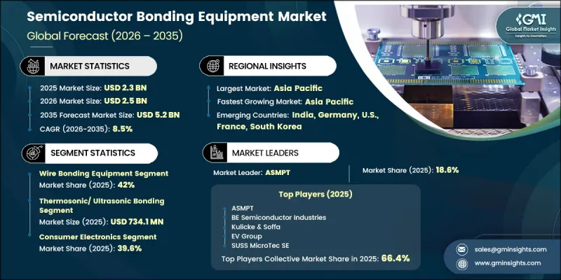
The Global Semiconductor Bonding Equipment Market was valued at USD 2.3 billion in 2025 and is estimated to grow at a CAGR of 8.5% to reach USD 5.2 billion by 2035.
Growth is supported by rising global fab capacity additions, rapid adoption of advanced nodes below 7nm, and increasing demand for heterogeneous integration and advanced packaging architectures. Strong investment momentum from artificial intelligence, high-performance computing, and data center chip production continues to reinforce equipment demand across front-end and back-end semiconductor processes. In parallel, government-led semiconductor localization programs are reshaping regional supply chains, encouraging domestic manufacturing expansion and reducing reliance on offshore production hubs. The ongoing transition toward 3D integration and chiplet-based designs is also intensifying the need for high-precision bonding technologies. Across fabrication ecosystems, packaging sophistication is increasing, requiring tighter interconnect density, improved thermal performance, and higher electrical efficiency, all of which directly elevate demand for advanced bonding equipment solutions across logic, memory, and specialty semiconductor applications.
| Market Scope | |
|---|---|
| Start Year | 2025 |
| Forecast Year | 2026-2035 |
| Start Value | $2.3 Billion |
| Forecast Value | $5.2 Billion |
| CAGR | 8.5% |
The wire bonding equipment segment accounted for 42% share in 2025. Its strong position is supported by extensive use in high-volume production environments where cost efficiency, throughput, and mature process reliability remain critical. This technology continues to be widely used in applications across automotive electronics, consumer devices, LED modules, power devices, and analog integrated circuits. Its adaptability across multiple packaging formats ensures continued relevance even as newer interconnect technologies emerge, particularly in configurations requiring scalable and cost-effective assembly solutions.
The hybrid bonding segment is expected to grow at a CAGR of 21.3% through 2035. Its rapid adoption is driven by the growing shift toward 3D integration and advanced heterogeneous packaging approaches. Copper-to-copper direct interconnection techniques are increasingly being adopted to achieve higher interconnect density, improved electrical performance, and reduced form factor. These capabilities are making hybrid bonding a key enabler for next-generation semiconductor architectures that require extreme miniaturization and performance optimization.
North America Semiconductor Bonding Equipment Market held 18.3% share in 2025. Regional growth is strongly influenced by large-scale semiconductor reshoring initiatives and government-backed investments aimed at expanding domestic packaging and assembly capabilities. Public funding programs supporting advanced packaging development are creating incremental demand for bonding equipment independent of wafer fabrication cycles, strengthening long-term installed base growth across the region.
The competitive landscape includes key industry participants such as Kulicke & Soffa, BE Semiconductor Industries, Shinkawa Ltd, Fasford Technology Co., Ltd, Hesse GmbH, F&K Delvotec Bondtechnik GmbH, KAIJO Corporation, Athlete FA Corporation, Micro Point Pro, F&S Bondtec Semiconductor GmbH, ASMPT, EV Group, SUSS MicroTec SE, Panasonic Connect Co., Ltd, Canon Machinery Inc, Toray Engineering Co., Ltd, and Shibuya Corporation. Companies in the semiconductor bonding equipment market are strengthening their market position by focusing on next-generation packaging solutions that support advanced node scaling and heterogeneous integration requirements. Manufacturers are increasing investment in hybrid and 3D bonding technologies to address rising demand for chiplet-based architectures and high-density interconnect solutions. Strategic collaborations with semiconductor foundries and OSAT providers are being prioritized to secure long-term equipment deployment contracts and co-development programs.
Table of Contents
Chapter 1 Methodology and Scope
- 1.1 Market scope and definition
- 1.2 Research design
- 1.2.1 Research approach
- 1.2.2 Data collection methods
- 1.3 Data mining sources
- 1.3.1 Global
- 1.3.2 Regional/Country
- 1.4 Base estimates and calculations
- 1.4.1 Base year calculation
- 1.4.2 Key trends for market estimation
- 1.5 Primary research and validation
- 1.5.1 Primary sources
- 1.6 Forecast model
- 1.7 Research assumptions and limitations
Chapter 2 Executive Summary
- 2.1 Industry 360° synopsis, 2022 - 2035
- 2.2 Key market trends
- 2.2.1 Equipment type trends
- 2.2.2 Bonding technology trends
- 2.2.3 Application trends
- 2.2.4 End-use industry trends
- 2.2.5 Regional trends
- 2.3 TAM Analysis, 2026-2035
- 2.4 CXO perspectives: Strategic imperatives
Chapter 3 Industry Insights
- 3.1 Industry ecosystem analysis
- 3.1.1 Supplier Landscape
- 3.1.2 Profit Margin
- 3.1.3 Cost structure
- 3.1.4 Value addition at each stage
- 3.1.5 Factor affecting the value chain
- 3.1.6 Disruptions
- 3.2 Industry impact forces
- 3.2.1 Growth drivers
- 3.2.1.1 Expansion of global semiconductor fabrication capacity and new fab construction
- 3.2.1.2 Transition to advanced process nodes below 7nm and EUV-based manufacturing
- 3.2.1.3 Rising adoption of advanced packaging and heterogeneous integration
- 3.2.1.4 Increasing semiconductor manufacturing localization and government-backed incentives
- 3.2.1.5 Growth in high-performance computing, AI, and data center chip production
- 3.2.2 Industry pitfalls and challenges
- 3.2.2.1 High capital intensity and long payback cycles of semiconductor equipment
- 3.2.2.2 Supply chain disruptions and dependence on critical sub-components
- 3.2.3 Market opportunities
- 3.2.3.1 Rising adoption of semiconductor equipment refurbishment and upgrade services
- 3.2.3.2 Expansion of semiconductor manufacturing in emerging regional hubs
- 3.2.1 Growth drivers
- 3.3 Growth potential analysis
- 3.4 Regulatory landscape
- 3.4.1 North America
- 3.4.2 Europe
- 3.4.3 Asia Pacific
- 3.4.4 Latin America
- 3.4.5 Middle East & Africa
- 3.5 Porter's analysis
- 3.6 PESTEL analysis
- 3.7 Technology and Innovation landscape
- 3.7.1 Current technological trends
- 3.7.2 Emerging technologies
- 3.8 Price trends
- 3.8.1 By region
- 3.8.2 By product
- 3.9 Pricing Strategies
- 3.10 Emerging Business Models
- 3.11 Compliance Requirements
- 3.12 Patent and IP analysis
Chapter 4 Competitive Landscape, 2025
- 4.1 Introduction
- 4.2 Company market share analysis
- 4.2.1 By region
- 4.2.1.1 North America
- 4.2.1.2 Europe
- 4.2.1.3 Asia Pacific
- 4.2.1.4 Latin America
- 4.2.1.5 Middle East & Africa
- 4.2.2 Market concentration analysis
- 4.2.1 By region
- 4.3 Competitive benchmarking of key players
- 4.3.1 Financial performance comparison
- 4.3.1.1 Revenue
- 4.3.1.2 Profit margin
- 4.3.1.3 R&D
- 4.3.2 Product portfolio comparison
- 4.3.2.1 Product range breadth
- 4.3.2.2 Technology
- 4.3.2.3 Innovation
- 4.3.3 Geographic presence comparison
- 4.3.3.1 Global footprint analysis
- 4.3.3.2 Service network coverage
- 4.3.3.3 Market penetration by region
- 4.3.4 Competitive positioning matrix
- 4.3.4.1 Leaders
- 4.3.4.2 Challengers
- 4.3.4.3 Followers
- 4.3.4.4 Niche players
- 4.3.5 Strategic outlook matrix
- 4.3.1 Financial performance comparison
- 4.4 Key developments
- 4.4.1 Mergers and acquisitions
- 4.4.2 Partnerships and collaborations
- 4.4.3 Technological advancements
- 4.4.4 Expansion and investment strategies
- 4.4.5 Digital transformation initiatives
- 4.5 Emerging/ startup competitors landscape
Chapter 5 Market Estimates and Forecast, By Equipment Type, 2022 - 2035 (USD Million)
- 5.1 Key trends
- 5.2 Wire bonding equipment
- 5.3 Die bonding equipment
- 5.3.1 Conventional die bonders
- 5.3.2 Flip-chip bonders
- 5.3.3 Advanced packaging die bonders
- 5.3.4 Pick-and-place / Die-picking equipment
- 5.4 Wafer bonding equipment
- 5.5 Hybrid bonding equipment
- 5.6 Others
- 5.7 By Bonding Technology
- 5.8 Thermocompression bonding
- 5.9 Thermosonic / ultrasonic bonding
- 5.10 Eutectic / solder bonding
- 5.11 Adhesive bonding
- 5.12 Fusion bonding
- 5.13 Anodic bonding
- 5.14 Hybrid bonding
- 5.15 Others
- 5.16 By Application
- 5.17 Logic devices
- 5.18 Memory devices
- 5.19 DRAM
- 5.20 NAND flash
- 5.21 High-bandwidth memory (HBM)
- 5.22 Semiconductor bonding equipments
- 5.23 MEMS devices
- 5.24 CMOS image sensors (CIS)
- 5.25 RF & microwave devices
- 5.26 Photonics & optoelectronics
- 5.27 Advanced sensor devices
- 5.28 Others
- 5.29 By End-Use Industry
- 5.30 Consumer electronics
- 5.31 Automotive
- 5.32 Data centers & high-performance computing (HPC)
- 5.33 Telecommunications
- 5.34 Industrial & automation
- 5.35 Healthcare & life sciences
- 5.36 Aerospace & defense
- 5.37 Others
Chapter 6 Market Estimates and Forecast, By Bonding Technology, 2022 - 2035 (USD Million)
- 6.1 Key trends
- 6.2 Thermocompression bonding
- 6.3 Thermosonic / ultrasonic bonding
- 6.4 Eutectic / solder bonding
- 6.5 Adhesive bonding
- 6.6 Fusion bonding
- 6.7 Anodic bonding
- 6.8 Hybrid bonding
- 6.9 Others
Chapter 7 Market Estimates and Forecast, By Application, 2022 - 2035 (USD Million)
- 7.1 Key trends
- 7.2 Logic devices
- 7.3 Memory devices
- 7.3.1 DRAM
- 7.3.2 NAND flash
- 7.3.3 High-bandwidth memory (HBM)
- 7.4 Semiconductor bonding equipments
- 7.5 MEMS devices
- 7.6 CMOS image sensors (CIS)
- 7.7 RF & microwave devices
- 7.8 Photonics & optoelectronics
- 7.9 Advanced sensor devices
- 7.10 Others
Chapter 8 Market Estimates and Forecast, By End-Use Industry, 2022 - 2035 (USD Million)
- 8.1 Key trends
- 8.2 Consumer electronics
- 8.3 Automotive
- 8.4 Data centers & high-performance computing (HPC)
- 8.5 Telecommunications
- 8.6 Industrial & automation
- 8.7 Healthcare & life sciences
- 8.8 Aerospace & defense
- 8.9 Others
Chapter 9 Market Estimates and Forecast, By Region, 2022 - 2035 (USD Million)
- 9.1 Key trends
- 9.2 North America
- 9.2.1 U.S.
- 9.2.2 Canada
- 9.3 Europe
- 9.3.1 Germany
- 9.3.2 UK
- 9.3.3 France
- 9.3.4 Spain
- 9.3.5 Italy
- 9.3.6 Russia
- 9.4 Asia Pacific
- 9.4.1 China
- 9.4.2 India
- 9.4.3 Japan
- 9.4.4 Australia
- 9.4.5 South Korea
- 9.5 Latin America
- 9.5.1 Brazil
- 9.5.2 Mexico
- 9.5.3 Argentina
- 9.6 Middle East and Africa
- 9.6.1 South Africa
- 9.6.2 Saudi Arabia
- 9.6.3 UAE
Chapter 10 Company Profiles
- 10.1 Global Key Players
- 10.1.1 ASMPT
- 10.1.2 BE Semiconductor Industries
- 10.1.3 Kulicke & Soffa
- 10.1.4 EV Group
- 10.1.5 SUSS MicroTec SE
- 10.2 Regional key players
- 10.2.1 North America
- 10.2.1.1 Micro Point Pro (MPP) Ltd
- 10.2.2 Asia Pacific
- 10.2.2.1 Shinkawa Ltd
- 10.2.2.2 Fasford Technology Co., Ltd
- 10.2.2.3 KAIJO Corporation
- 10.2.2.4 Athlete FA Corporation
- 10.2.2.5 Panasonic Connect Co., Ltd
- 10.2.2.6 Canon Machinery Inc
- 10.2.2.7 Toray Engineering Co., Ltd
- 10.2.2.8 Shibuya Corporation
- 10.2.3 Europe
- 10.2.3.1 Hesse GmbH
- 10.2.3.2 F&K Delvotec Bondtechnik GmbH
- 10.2.3.3 F&S Bondtec Semiconductor GmbH
- 10.2.1 North America

