
PUBLISHER: Mordor Intelligence | PRODUCT CODE: 2035144

PUBLISHER: Mordor Intelligence | PRODUCT CODE: 2035144
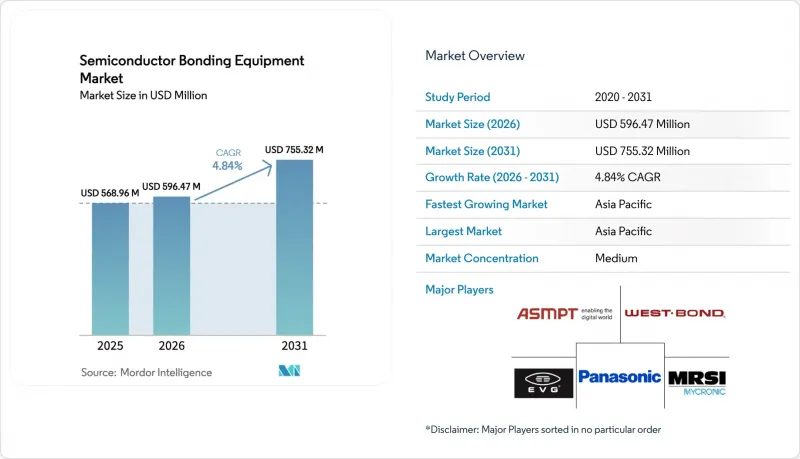
Semiconductor Bonding Equipment - Market Share Analysis, Industry Trends & Statistics, Growth Forecasts (2026 - 2031)
The semiconductor bonding equipment market size in 2026 is estimated at USD 596.47 million, growing from 2025 value of USD 568.96 million with 2031 projections showing USD 755.32 million, growing at 4.84% CAGR over 2026-2031.
Demand growth mirrors the industry shift from planar scaling to vertical stacking, where heterogeneous integration strategies require precise wafer-to-wafer and die-to-wafer connections. Leading chipmakers have accelerated capital spending on advanced packaging lines to improve bandwidth, latency, and energy efficiency for AI accelerators and high-performance computing devices. Hybrid copper-to-copper processes are eclipsing conventional wire bonding as sub-3 nm nodes move into risk production, raising alignment-accuracy demands below 10 µm. At the same time, automotive electrification and IoT miniaturization widen the application footprint, expanding order books for permanent, temporary, and hybrid platforms. However, the high total cost of ownership and tighter environmental rules on volatile organic compounds add pressure to sustain utilization levels above 70%, prompting buyers to negotiate full-service contracts and predictive-maintenance packages.
Global Semiconductor Bonding Equipment Market Trends and Insights
Increasing CAPEX by IDMs and Foundries
Global semiconductor equipment spending hit USD 110 billion in 2024 and is on track for USD 130 billion by 2026. TSMC alone earmarked USD 38-42 billion for 2025 facility upgrades, a substantial portion of which funds advanced packaging and bonding lines. Comparable expansions by Samsung and Intel emphasize the competitive need for wafer-level integration that supports high-bandwidth memory and chiplet designs. Capital allocation now targets line items such as sub-micrometer optical alignment modules, vacuum bond chambers, and AI-enabled process control. Vendors that provide modular upgrade paths are gaining preferred-supplier status as device makers hedge against future design pivots. The investment uptick stimulates the semiconductor bonding equipment market by shortening replacement cycles and broadening the installed base across both front-end and back-end fabs.
Surging Semiconductor Content in Automotive and IoT Devices
Average semiconductor value per vehicle climbed to USD 950 in 2024, driven by electrified powertrains, advanced driver-assistance systems, and zonal architectures. Electric models specify silicon-carbide and gallium-nitride power devices that need high-force, high-temperature bonding heads and robust flux-management systems. In parallel, IoT wearables and smart home nodes demand wafer-level chip-scale packages that shrink footprint and extend battery life. These divergent requirements converge at the equipment level, where configurable bonders must toggle between high-power pressure profiles and delicate MEMS handling. Suppliers are addressing the gap with adaptive clamp designs, real-time chuck-planarity feedback, and recipe-driven force curves. The trend raises unit shipments in the semiconductor bonding equipment market while diversifying revenue streams across automotive Tier-1s and consumer OEMs.
High Cost of Ownership and TCO Uncertainty
State-of-the-art hybrid bonders list above USD 3 million, while annual running costs including spares, consumables, and calibration can lift lifetime spend to USD 8 million. Smaller OSATs struggle when utilization drifts below 70%, especially in consumer-electronics off-seasons. Rapid roadmap updates further complicate financial modeling because a tool qualified for 10 µm overlay may need retrofit kits after only two product cycles. Leasing programs, outcome-based service contracts, and shared-risk pricing models are emerging, yet CFOs still cite uncertain residual value as a brake on new orders within the semiconductor bonding equipment market.
Other drivers and restraints analyzed in the detailed report include:
- Rapid Adoption of Advanced 2.5D/3D Packaging Platforms
- Government-Backed "CHIPS" Subsidies and Tax Incentives
- Process Complexity at Sub-10 µm Alignment Tolerances
For complete list of drivers and restraints, kindly check the Table Of Contents.
Segment Analysis
Permanent bonders accounted for 38.74% of 2025 revenue, underpinned by their proven reliability in legacy device packaging. Temporary bonding tools cater to wafer thinning and TSV creation, providing the reversible adhesion needed for mechanical support. Hybrid systems register the quickest climb at 5.88% CAGR, targeting sub-3 nm integration where copper-to-copper direct attach minimizes resistance and electromigration. That growth lifts the semiconductor bonding equipment market size for hybrid platforms from a modest base toward parity with permanent tools before the decade closes. Manufacturers differentiate through dual-stage alignment optics, active levelling chucks, and closed-loop pressure control that collectively push placement error below 500 nm. Buyers favor multi-modal units that accept future recipe add-ons, lowering capital risk. The pivot intensifies R&D around heat-spreader materials and compliant under-fill chemistries that withstand repeated thermal cycles without delamination. Competition also hinges on throughput, with flagship machines now promising 20% cycle-time reductions achieved via parallel clamp arms and predictive servo tuning.
A broader equipment refresh cycle accompanies the shift. Line managers audited older eutectic stations and discovered maintenance outlays rising 12% per year. Swapping to hybrid bonders eliminates dual-pass processes, improving floor utilization. Yet stakeholders insist that new gear integrate seamlessly with MES and factory automation layers that handle traceability down to die serial number. Vendors respond by embedding OPC-UA gateways and edge analytics that channel process data into AI-based yield dashboards. Such ecosystem compatibility accelerates factory-wide adoption, reinforcing the hybrid segment's contribution to the semiconductor bonding equipment market.
Advanced packaging maintained 35.42% of 2025 revenue and remains the anchor segment, buttressed by chiplet processors, high-bandwidth memory, and premium smartphone SoC programs. Power IC bonding, while less glamorous, delivers stable volumes that depend on rigorous void-control protocols and high-pressure thermocompression heads. Silicon photonics is the standout high-velocity niche at a 5.73% CAGR. Optical engines co-packaged with switch ASICs need micron-accurate placement of germanium photodetectors and III-V lasers onto silicon carrier wafers, driving specialized bond recipes with controlled temperature ramps under 250 °C. The strong demand trajectory has already lifted the silicon-photonics slice from single digits toward a double-digit share of the overall semiconductor bonding equipment market size.
MEMS sensors, notably for automotive lidar and industrial automation, require hermetic seals that endure 1,000-cycle temperature swings. These stress profiles favor glass-frit or anodic bonding, sustaining a market foothold for niche tool vendors. CMOS image sensors push alignment fidelity to safeguard optical axis integrity, stoking orders for advanced auto-focus optics built into bond heads. RF devices, meanwhile, introduce unique impedances that compel low-loss interconnect metallurgy, influencing material-delivery subsystems on next-gen machines. The blend of widespread and emerging uses buffers suppliers from cyclical swings and keeps the semiconductor bonding equipment market on a stable growth path.
The Semiconductor Bonding Equipment Market Report is Segmented by Equipment Type (Permanent, Temporary, and Hybrid), Application (Advanced Packaging, Power IC and Discrete, and More), Bonding Technology (Thermocompression, Eutectic/Solder, and More), Wafer Size (<=200mm, and More), End User (IDMs, Foundries, and OSAT), and Geography (North America, Europe, and More). The Market Forecasts are Provided in Terms of Value (USD).
Geography Analysis
Asia-Pacific held 52.64% of 2025 revenue, underlined by USD 49.6 billion in equipment spending from China alone, up 35% year over year. South Korea followed with USD 20.5 billion, and Taiwan contributed USD 16.6 billion despite temporary inventory corrections. Regional policy packages include tax deductions, duty exemptions, and infrastructure subsidies that lower effective purchase prices of hybrid bonders, sustaining leadership in the semiconductor bonding equipment market. Local champions such as TSMC and Samsung spearhead 3D and hybrid adoption, elevating regional technical standards and reshaping supply-chain expectations for precision chucks and ultra-flat carrier wafers.
North America posted USD 13.7 billion in 2024 sales, advancing 14% alongside CHIPS Act allocations targeting domestic capacity expansion. Intel, Micron, and Texas Instruments have announced multiyear packaging projects anchored in Arizona, Ohio, and Texas. The subsidy stimulus accelerates inbound orders but raises concerns over long-term cost competitiveness once grants taper. Yet the region benefits from proximity to hyperscale-data-center customers demanding low-latency interposers for AI workloads, a segment that outlets more value-added hybrid bonders into the semiconductor bonding equipment market. Europe concentrates spending in Germany and the Netherlands where analog, power, and EUV tool vendors cluster. Collaborative programs like IPCEI-ME/CT channel EUR funding into 3D integration, especially for automotive power modules that require stringent reliability. Middle East and Africa remain nascent, though Saudi Arabia's Vision 2030 and the UAE's strategic tech funds have earmarked pilot lines for compound semiconductors. These early moves hint at wider regional diversification that could incrementally enlarge the semiconductor bonding equipment market beyond its traditional APAC stronghold.,
- EV Group (EVG)
- ASMPT Semiconductor Solutions
- Mycronic AB (MRSI Systems)
- WestBond, Inc.
- Panasonic Holdings Corporation
- Palomar Technologies, Inc.
- Dr. Tresky AG
- BE Semiconductor Industries N.V.
- Fasford Technology Co., Ltd.
- Kulicke & Soffa Industries, Inc.
- DIAS Automation (HK) Ltd.
- Shibaura Mechatronics Corporation
- SUSS MicroTec SE
- Tokyo Electron Limited
- DISCO Corporation
- TOWA Corporation
- Hanmi Semiconductor Co., Ltd.
- Toray Engineering Co., Ltd.
- Hesse GmbH
- Finetech GmbH & Co. KG
Additional Benefits:
- The market estimate (ME) sheet in Excel format
- 3 months of analyst support
TABLE OF CONTENTS
1 INTRODUCTION
- 1.1 Study Assumptions and Market Definition
- 1.2 Scope of the Study
2 RESEARCH METHODOLOGY
3 EXECUTIVE SUMMARY
4 MARKET LANDSCAPE
- 4.1 Market Overview
- 4.2 Market Drivers
- 4.2.1 Increasing CAPEX by IDMs and foundries
- 4.2.2 Surging semiconductor content in automotive and IoT devices
- 4.2.3 Rapid adoption of advanced 2.5D/3D packaging platforms
- 4.2.4 Government-backed "CHIPS" subsidies and tax incentives
- 4.2.5 Commercial roll-out of hybrid wafer-to-wafer bonding in CIS and 3D-NAND
- 4.2.6 Silicon-photonic interposers for AI datacenters driving wafer bonding tools
- 4.3 Market Restraints
- 4.3.1 High cost of ownership and TCO uncertainty
- 4.3.2 Process complexity at sub-10 µm alignment tolerances
- 4.3.3 Supply-chain bottlenecks for ultra-flat carrier wafers
- 4.3.4 Stricter VOC / adhesive-chemistry environmental regulations
- 4.4 Industry Value Chain Analysis
- 4.5 Regulatory Landscape
- 4.6 Technological Outlook
- 4.7 Porter's Five Forces Analysis
- 4.7.1 Bargaining Power of Suppliers
- 4.7.2 Bargaining Power of Buyers
- 4.7.3 Threat of New Entrants
- 4.7.4 Threat of Substitutes
- 4.7.5 Intensity of Competitive Rivalry
- 4.8 Impact of Macroeconomic Factors on the Market
5 MARKET SIZE AND GROWTH FORECASTS (VALUE)
- 5.1 By Equipment Type
- 5.1.1 Permanent Bonding Equipment
- 5.1.2 Temporary Bonding Equipment
- 5.1.3 Hybrid Bonding Equipment
- 5.2 By Application
- 5.2.1 Advanced Packaging
- 5.2.2 Power IC and Discrete
- 5.2.3 Photonic Devices
- 5.2.4 MEMS Sensors and Actuators
- 5.2.5 Engineered Substrates
- 5.2.6 RF Devices
- 5.2.7 CMOS Image Sensors
- 5.3 By Bonding Technology
- 5.3.1 Thermocompression Bonding
- 5.3.2 Eutectic/Solder Bonding
- 5.3.3 Adhesive/Polymer Bonding
- 5.3.4 Ultrasonic / Thermosonic Bonding
- 5.3.5 Anodic / Fusion Bonding
- 5.4 By Wafer Size
- 5.4.1 Less than equal to 200 mm
- 5.4.2 200-300 mm
- 5.4.3 Greater than 300 mm
- 5.5 By End User
- 5.5.1 Integrated Device Manufacturers (IDMs)
- 5.5.2 Foundries
- 5.5.3 Outsourced Semiconductor Assembly and Test (OSAT)
- 5.6 Geography
- 5.6.1 North America
- 5.6.1.1 United States
- 5.6.1.2 Rest of North America
- 5.6.2 South America
- 5.6.3 Europe
- 5.6.3.1 Germany
- 5.6.3.2 France
- 5.6.3.3 Rest of Europe
- 5.6.4 Asia-Pacific
- 5.6.4.1 China
- 5.6.4.2 Japan
- 5.6.4.3 South Korea
- 5.6.4.4 India
- 5.6.4.5 Rest of Asia-Pacific
- 5.6.5 Middle East
- 5.6.6 Africa
- 5.6.1 North America
6 COMPETITIVE LANDSCAPE
- 6.1 Market Concentration
- 6.2 Strategic Moves
- 6.3 Market Share Analysis
- 6.4 Company Profiles (includes Global level Overview, Market level overview, Core Segments, Financials as available, Strategic Information, Market Rank/Share for key companies, Products and Services, and Recent Developments)
- 6.4.1 EV Group (EVG)
- 6.4.2 ASMPT Semiconductor Solutions
- 6.4.3 Mycronic AB (MRSI Systems)
- 6.4.4 WestBond, Inc.
- 6.4.5 Panasonic Holdings Corporation
- 6.4.6 Palomar Technologies, Inc.
- 6.4.7 Dr. Tresky AG
- 6.4.8 BE Semiconductor Industries N.V.
- 6.4.9 Fasford Technology Co., Ltd.
- 6.4.10 Kulicke & Soffa Industries, Inc.
- 6.4.11 DIAS Automation (HK) Ltd.
- 6.4.12 Shibaura Mechatronics Corporation
- 6.4.13 SUSS MicroTec SE
- 6.4.14 Tokyo Electron Limited
- 6.4.15 DISCO Corporation
- 6.4.16 TOWA Corporation
- 6.4.17 Hanmi Semiconductor Co., Ltd.
- 6.4.18 Toray Engineering Co., Ltd.
- 6.4.19 Hesse GmbH
- 6.4.20 Finetech GmbH & Co. KG
7 MARKET OPPORTUNITIES AND FUTURE OUTLOOK
- 7.1 White-space and Unmet-need Assessment

