
PUBLISHER: MarketsandMarkets | PRODUCT CODE: 1889161

PUBLISHER: MarketsandMarkets | PRODUCT CODE: 1889161
Hybrid Bonding Market by Packaging Architecture (Wafer-to-Wafer, Die-to-Wafer, Die-to-Die ), Equipment Type, Integration level - Global Forecast to 2032
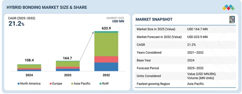
The global hybrid bonding market is expected to reach USD 164.7 million in 2025 and USD 633.9 million by 2032, recording a CAGR of 21.2% from 2025 to 2032. Global hybrid bonding adoption is accelerating as semiconductor manufacturers transition to 3D integration to overcome scaling limitations and achieve higher bandwidth, lower latency, and improved power efficiency.
| Scope of the Report | |
|---|---|
| Years Considered for the Study | 2020-2032 |
| Base Year | 2024 |
| Forecast Period | 2025-2032 |
| Units Considered | Value (USD Billion) |
| Segments | By Packaging Architecture, Process Flow, Equipment Type and region |
| Regions covered | North America, Europe, APAC, RoW |
The rise of chiplet-based architectures in AI, HPC, and advanced logic devices further strengthens the need for ultra-fine-pitch interconnects that hybrid bonding enables. Continued investments in advanced packaging capacity by leading foundries and IDMs, combined with increasing requirements for compact, high-performance electronics, are reinforcing strong market momentum worldwide.
"Wafer-to-wafer (W2W) segment accounted for the largest market share in 2024."
The wafer-to-wafer (W2W) segment held the largest share of the hybrid bonding market in 2024 as it provides the highest level of process uniformity, alignment accuracy, and throughput, making it ideal for large-scale production environments. Major memory manufacturers and foundries rely heavily on W2W processes for 3D NAND, DRAM stacking, and CIS manufacturing, where consistent wafer-level bonding is essential to achieving high yields. Its capability to support extremely fine-pitch interconnects across full wafers also reduces overall manufacturing complexity compared to die-level approaches. As leading semiconductor fabs continue expanding 3D integration capacity, W2W remains the foundation of most high-volume hybrid bonding deployments.
"Computing & logic segment is projected to witness the highest CAGR in the hybrid bonding market from 2025 to 2032."
Computing & logic applications are expected to grow the fastest during the forecast period due to the demand for high-performance AI accelerators, HPC processors, data-center workloads, and advanced edge computing systems. Hybrid bonding enables the ultra-dense vertical interconnects these devices require to achieve higher bandwidth, improved energy efficiency, and tighter logic-to-memory integration. The rapid industry shift toward chiplet-based designs further boosts adoption, as hybrid bonding helps overcome reticle-size limits and enhances scalability. With continuous investments in next-generation logic architectures and multi-die packaging, the computing and logic segment is positioned for the strongest growth trajectory.
"India is expected to record the highest CAGR in the Asia Pacific hybrid bonding market from 2025 to 2032."
India is expected to exhibit the highest CAGR in Asia Pacific during the forecast period due to its rapid expansion of semiconductor manufacturing and advanced packaging initiatives supported by strong government incentives and policy frameworks. Large-scale investments under national semiconductor missions accelerate the development of new fabs, OSAT facilities, and research centers focused on 3D integration and hybrid bonding-related capabilities. The country also witnesses the rising demand for high-performance electronics across telecom, automotive, and data-center sectors, which drives the need for advanced packaging technologies. Combined with increasing collaboration with global equipment suppliers and technology partners, the country is positioned for the fastest growth in hybrid bonding adoption in the region.
Extensive primary interviews were conducted with key industry experts in the hybrid bonding market space to determine and verify the market size for various segments and subsegments gathered through secondary research. The breakdown of primary participants for the report is shown below:
The study contains insights from various industry experts, from component suppliers to Tier 1 companies and OEMs. The break-up of the primaries is as follows:
- By Company Type: Tier 1 - 35%, Tier 2 - 45%, and Tier 3 - 20%
- By Designation: C-level Executives - 40%, Managers - 30%, and Others - 30%
- By Region: North America - 40%, Europe - 30%, Asia Pacific - 20%, and RoW - 10%
Daifuku Co., Ltd. (Japan), MURATA MACHINERY, LTD. (Japan), Exyte Group (Germany), DuPont (US), and Thermo Fisher Scientific Inc. (US) are some key players in the hybrid bonding market.
Research Coverage:
This research report categorizes the hybrid bonding market based on Packaging Architecture [Wafer-to-Wafer (W2W), Die-to-Wafer (D2W), and Die-to-Die (D2D)], Process Flow (Front-end and Back-end), Equipment Type (Wafer Bonders, Cleaning & CMP Systems, Surface Prep Tools, and Inspection & Metrology Tools), Bonding Type [Copper-to-copper (Cu-Cu), Copper-to-pad/metal-to-pad, and Other Bonding Types], Integration Level (2.5D Packaging with Hybrid Bonding, 3D Stacked ICs, and Heterogeneous Integration), Application (Computing & Logic, Memory & Storage, Sensing & Interface, Connectivity & Communications, and Other Applications) Vertical (IT & Telecommunications, Consumer Electronics, Automotive, Aerospace & Defense, Healthcare & Medical, Industrial Automation, and Other Verticals), and Region (North America, Europe, Asia Pacific, and RoW). The report describes the major drivers, restraints, challenges, and opportunities pertaining to the hybrid bonding market and forecasts the same till 2030. Apart from this, the report also consists of leadership mapping and analysis of all the companies included in the hybrid bonding ecosystem.
Key Benefits of Buying the Report
The report will help the market leaders/new entrants in this market by providing information on the closest approximations of the revenue numbers for the overall hybrid bonding market and the subsegments. This report will help stakeholders to understand the competitive landscape and gain more insights to position their businesses better and plan suitable go-to-market strategies. The report also helps stakeholders understand the pulse of the market and provides them with information on key market drivers, restraints, challenges, and opportunities.
The report provides insights into the following pointers:
- Analysis of key drivers (Rising demand for high-bandwidth, low-latency interconnects in AI, HPC, and logic-memory systems, Increasing reliance on advanced hybrid bonding to power >200-layer 3D memory, Shift toward chiplet-based architectures to overcome reticle limits and reduce system power, Growing need for low-temperature bonding to support fragile materials, advanced BEOL stacks, and next-gen devices), restraints (Substantial upfront capital investment and Stringent environment and surface quality requirements), opportunities (Rising need for ultra-dense logic-to-memory connectivity in AI/ML accelerators and Deployment of hybrid bonding in CIS and AR/VR sensors to improve SNR and pixel density), and challenges (Issues in maintaining ultra-low defectivity across wafers and Lack of standardization in die formats, pad structures, and surface pre-treatment flows) influencing the growth of the hybrid bonding market
- Product Development/Innovation: Detailed insights on upcoming technologies, research & development activities, and new product launches in the hybrid bonding market
- Market Development: Comprehensive information about lucrative markets-the report analyzes the hybrid bonding market across varied regions
- Market Diversification: Exhaustive information about new products, untapped geographies, recent developments, and investments in the hybrid bonding market
- Competitive Assessment: In-depth assessment of market shares, growth strategies, and product offerings of leading players, including EV Group (EVG) (Austria), Applied Materials, Inc. (US), SUSS MicroTec SE (Germany), Besi (Netherlands), Kulicke & Soffa Industries, Inc. (Singapore), Tokyo Electron (TEL) (Japan), ASMPT (Singapore), Lam Research Corporation (US), and SHIBAURA MECHATRONICS CORPORATION (Japan), in the hybrid bonding market
TABLE OF CONTENTS
1 INTRODUCTION
- 1.1 STUDY OBJECTIVES
- 1.2 MARKET DEFINITION
- 1.3 STUDY SCOPE
- 1.3.1 MARKET SEGMENTATION AND REGIONAL SCOPE
- 1.3.2 INCLUSIONS AND EXCLUSIONS
- 1.3.3 YEARS CONSIDERED
- 1.4 CURRENCY CONSIDERED
- 1.5 UNIT CONSIDERED
- 1.6 LIMITATIONS
- 1.7 STAKEHOLDERS
2 EXECUTIVE SUMMARY
- 2.1 MARKET HIGHLIGHTS AND KEY INSIGHTS
- 2.2 KEY MARKET PARTICIPANTS: MAPPING OF STRATEGIC DEVELOPMENTS
- 2.3 DISRUPTIVE TRENDS IN HYBRID BONDING MARKET
- 2.4 HIGH-GROWTH SEGMENTS
- 2.5 REGIONAL SNAPSHOT: MARKET SIZE, GROWTH RATE, AND FORECAST
3 PREMIUM INSIGHTS
- 3.1 ATTRACTIVE OPPORTUNITIES FOR PLAYERS IN HYBRID BONDING MARKET
- 3.2 HYBRID BONDING MARKET, BY PACKAGING ARCHITECTURE
- 3.3 HYBRID BONDING MARKET, BY PROCESS FLOW
- 3.4 HYBRID BONDING MARKET, BY APPLICATION
- 3.5 HYBRID BONDING MARKET, BY VERTICAL
- 3.6 HYBRID BONDING MARKET, BY REGION
4 MARKET OVERVIEW
- 4.1 INTRODUCTION
- 4.2 MARKET DYNAMICS
- 4.2.1 DRIVERS
- 4.2.1.1 Rising demand for high-bandwidth, low-latency interconnects in AI, HPC, and logic-memory systems
- 4.2.1.2 Increasing reliance on advanced hybrid bonding to power >200-layer 3D memory
- 4.2.1.3 Shift toward chiplet-based architectures to overcome reticle limits and reduce system power
- 4.2.1.4 Growing need for low-temperature bonding to support fragile materials, advanced BEOL stacks, and next-gen devices
- 4.2.2 RESTRAINTS
- 4.2.2.1 Substantial upfront capital investment
- 4.2.2.2 Stringent environment and surface quality requirements
- 4.2.3 OPPORTUNITIES
- 4.2.3.1 Rising need for ultra-dense logic-to-memory connectivity in AI/ML accelerators
- 4.2.3.2 Deployment of hybrid bonding in CIS and AR/VR sensors to improve SNR and pixel density
- 4.2.4 CHALLENGES
- 4.2.4.1 Issues in maintaining ultra-low defectivity across wafers
- 4.2.4.2 Lack of standardization in die formats, pad structures, and surface pre-treatment flows
- 4.2.1 DRIVERS
- 4.3 UNMET NEEDS AND WHITE SPACES
- 4.4 INTERCONNECTED MARKETS AND CROSS-SECTOR OPPORTUNITIES
- 4.5 STRATEGIC MOVES BY TIER-1/2/3 PLAYERS
5 INDUSTRY TRENDS
- 5.1 PORTER'S FIVE FORCES ANALYSIS
- 5.1.1 INTENSITY OF COMPETITIVE RIVALRY
- 5.1.2 BARGAINING POWER OF SUPPLIERS
- 5.1.3 BARGAINING POWER OF BUYERS
- 5.1.4 THREAT OF SUBSTITUTES
- 5.1.5 THREAT OF NEW ENTRANTS
- 5.2 MACROECONOMIC OUTLOOK
- 5.2.1 INTRODUCTION
- 5.2.2 GDP TRENDS AND FORECAST
- 5.2.3 TRENDS IN GLOBAL SEMICONDUCTOR MANUFACTURING EQUIPMENT INDUSTRY
- 5.2.4 TRENDS IN GLOBAL SEMICONDUCTOR INSPECTION AND METROLOGY INDUSTRY
- 5.3 SUPPLY CHAIN ANALYSIS
- 5.4 ECOSYSTEM ANALYSIS
- 5.5 PRICING ANALYSIS
- 5.5.1 AVERAGE SELLING PRICE OF WAFER BONDERS, BY KEY PLAYER, 2024
- 5.5.2 AVERAGE SELLING PRICE OF WAFER BONDERS, BY REGION, 2024
- 5.6 TRADE ANALYSIS
- 5.6.1 IMPORT SCENARIO (HS CODE 848620)
- 5.6.2 EXPORT SCENARIO (HS CODE 848620)
- 5.7 KEY CONFERENCES AND EVENTS, 2025-2026
- 5.8 TRENDS/DISRUPTIONS IMPACTING CUSTOMER BUSINESS
- 5.9 INVESTMENT AND FUNDING SCENARIO
- 5.10 CASE STUDY ANALYSIS
- 5.10.1 IMEC PARTNERS WITH EV GROUP TO DEVELOP ADVANCED PROCESS FLOWS TO ACHIEVE FINE-PITCH INTERCONNECTS
- 5.10.2 SUSS MICROTEC INTRODUCES XBC300 GEN2 TO ENABLE WAFER-TO-WAFER AND DIE-TO-WAFER BONDING IN INNOVATION CENTERS AND SEMICONDUCTOR PILOT LINES
- 5.10.3 APPLIED MATERIALS AND BESI DELIVER INTEGRATED D2W HYBRID BONDING TO SUPPORT HIGH-VOLUME MANUFACTURING
- 5.11 IMPACT OF 2025 US TARIFF - HYBRID BONDING MARKET
- 5.11.1 INTRODUCTION
- 5.11.2 KEY TARIFF RATES
- 5.11.3 PRICE IMPACT ANALYSIS
- 5.11.4 IMPACT ON COUNTRIES/REGIONS
- 5.11.4.1 US
- 5.11.4.2 Europe
- 5.11.4.3 Asia Pacific
- 5.11.5 IMPACT ON VERTICALS
6 TECHNOLOGICAL ADVANCEMENTS, AI-DRIVEN IMPACTS, PATENTS, INNOVATIONS, AND FUTURE APPLICATIONS
- 6.1 KEY EMERGING TECHNOLOGIES
- 6.1.1 SUB-MICRON AND DIRECT CU-TO-CU HYBRID BONDING
- 6.1.2 LOW-TEMPERATURE HYBRID BONDING (<200°C)
- 6.2 COMPLEMENTARY TECHNOLOGIES
- 6.2.1 ADVANCED CMP
- 6.3 TECHNOLOGY/PRODUCT ROADMAP
- 6.4 PATENT ANALYSIS
- 6.5 IMPACT OF AI/GEN AI ON HYBRID BONDING MARKET
- 6.5.1 TOP USE CASES AND MARKET POTENTIAL
- 6.5.2 BEST PRACTICES FOLLOWED BY OEMS IN HYBRID BONDING MARKET
- 6.5.3 CASE STUDIES RELATED TO AI IMPLEMENTATION IN HYBRID BONDING MARKET
- 6.5.4 INTERCONNECTED ECOSYSTEM AND IMPACT ON MARKET PLAYERS
- 6.5.5 CLIENTS' READINESS TO ADOPT AI-INTEGRATED HYBRID BONDING SOLUTIONS
7 REGULATORY LANDSCAPE AND SUSTAINABILITY INITIATIVES
- 7.1 REGIONAL REGULATIONS AND COMPLIANCE
- 7.1.1 REGULATORY BODIES, GOVERNMENT AGENCIES, AND OTHER ORGANIZATIONS
- 7.1.2 INDUSTRY STANDARDS
- 7.2 SUSTAINABILITY INITIATIVES
- 7.3 IMPACT OF REGULATORY POLICIES ON SUSTAINABILITY INITIATIVES
- 7.4 CERTIFICATIONS, LABELING, AND ECO-STANDARDS
8 CUSTOMER LANDSCAPE AND BUYER BEHAVIOR
- 8.1 DECISION-MAKING PROCESS
- 8.2 KEY STAKEHOLDERS INVOLVED IN BUYING PROCESS AND THEIR EVALUATION CRITERIA
- 8.2.1 KEY STAKEHOLDERS IN BUYING PROCESS
- 8.2.2 BUYING CRITERIA
- 8.3 ADOPTION BARRIERS AND INTERNAL CHALLENGES
- 8.4 UNMET NEEDS OF VARIOUS VERTICALS
9 MATERIALS FOR HYBRID BONDING
- 9.1 INTRODUCTION
- 9.2 BONDING MATERIALS (OXIDE LAYERS, COPPER, AND METALLIZATION STACKS)
- 9.3 ADHESIVES AND TEMPORARY BONDING MATERIALS
- 9.4 CLEANING AND SURFACE PREPARATION MATERIALS
10 HYBRID BONDING MARKET, BY BONDING TYPE
- 10.1 INTRODUCTION
- 10.2 COPPER-TO-COPPER (CU-CU)
- 10.2.1 DEMAND FOR HIGH-PERFORMANCE INTERCONNECTS AT FINE PITCHES TO DRIVE MARKET
- 10.3 COPPER-TO-PAD/METAL-TO-PAD
- 10.3.1 NEED FOR PROCESS FLEXIBILITY AND COMPATIBILITY WITH DIVERSE METALLIZATION SCHEMES TO FUEL SEGMENTAL GROWTH
- 10.4 OTHER BONDING TYPES
11 HYBRID BONDING MARKET, BY PACKAGING ARCHITECTURE
- 11.1 INTRODUCTION
- 11.2 WAFER-TO-WAFER (W2W)
- 11.2.1 HIGH THROUGHPUT, PITCH SCALABILITY, AND COST EFFICIENCY FOR HOMOGENEOUS HIGH-VOLUME STACKS TO SPUR DEMAND
- 11.3 DIE-TO-WAFER (D2W)
- 11.3.1 YIELD OPTIMIZATION AND HETEROGENEOUS COMPONENT INTEGRATION TO BOLSTER SEGMENTAL GROWTH
- 11.4 DIE-TO-DIE (D2D)
- 11.4.1 FOCUS ON MODULARITY, LATENCY REDUCTION, AND POWER EFFICIENCY OF COMPUTE ARCHITECTURES TO BOOST SEGMENTAL GROWTH
12 HYBRID BONDING MARKET, BY INTEGRATION LEVEL
- 12.1 INTRODUCTION
- 12.2 2.5D PACKAGING
- 12.2.1 NEED FOR HIGH-BANDWIDTH INTERCONNECTS AND IMPROVED SIGNAL INTEGRITY IN LATERAL DIE CONFIGURATIONS TO DRIVE MARKET
- 12.3 3D STACKED ICS
- 12.3.1 RISING ADOPTION OF STACKED COMPUTE TILES IN HPC AND DATA CENTER PROCESSORS TO FOSTER SEGMENTAL GROWTH
- 12.4 HETEROGENEOUS INTEGRATION
- 12.4.1 SUPPORT FOR ADVANCED SURFACE ACTIVATION, HIGH-ACCURACY DIE PLACEMENT, WARPAGE CONTROL, AND LOW-TEMPERATURE BONDING TO SPUR DEMAND
13 HYBRID BONDING MARKET, BY PROCESS FLOW
- 13.1 INTRODUCTION
- 13.2 BACK-END
- 13.2.1 FOCUS ON CREATING DENSE, LOW-LATENCY INTERCONNECTS AT PACKAGING LEVEL TO ACCELERATE SEGMENTAL GROWTH
- 13.3 FRONT-END
- 13.3.1 NEED FOR HIGH INTERCONNECT PERFORMANCE AND INTEGRATION PRECISION TO AUGMENT SEGMENTAL GROWTH
14 HYBRID BONDING MARKET, BY EQUIPMENT TYPE
- 14.1 INTRODUCTION
- 14.2 WAFER BONDERS
- 14.2.1 NEED FOR SUB-MICRON ALIGNMENT, ULTRA-FLAT SURFACES, AND LOW-TEMPERATURE CU-CU DIFFUSION BONDING TO FUEL SEGMENTAL GROWTH
- 14.3 SURFACE PREPARATION TOOLS
- 14.3.1 ABILITY TO SUPPORT PLASMA ACTIVATION, ION-BEAM CLEANING, AND CHEMICAL SURFACE CONDITIONING TO CONTRIBUTE TO SEGMENTAL GROWTH
- 14.4 INSPECTION & METROLOGY TOOLS
- 14.4.1 SUB-MICRON OVERLAY MEASUREMENT, VOID DETECTION, AND POST-BOND VERIFICATION ATTRIBUTES TO FOSTER SEGMENTAL GROWTH
- 14.5 CLEANING & CMP SYSTEMS
- 14.5.1 ABILITY TO PROVIDE PLANARIZED COPPER/DIELECTRIC LAYERS AND CONTAMINANT-FREE SURFACES TO BOLSTER SEGMENTAL GROWTH
15 HYBRID BONDING MARKET, BY APPLICATION
- 15.1 INTRODUCTION
- 15.2 COMPUTING & LOGIC
- 15.2.1 HIGH-PERFORMANCE COMPUTING (HPC) & AI ACCELERATORS
- 15.2.1.1 Requirement for massive bandwidth scaling, fine-grained parallelism, and data locality optimization to drive market
- 15.2.2 HETEROGENEOUS SOCS & CHIPLET INTEGRATION
- 15.2.2.1 Extremely dense, short-reach links of chip architectures to contribute to segmental growth
- 15.2.1 HIGH-PERFORMANCE COMPUTING (HPC) & AI ACCELERATORS
- 15.3 MEMORY & STORAGE
- 15.3.1 HIGH-BANDWIDTH MEMORY (HBM)
- 15.3.1.1 Increasing demand for multi-terabit bandwidth between GPUs/AI accelerators and memory stacks to boost segmental growth
- 15.3.2 3D NAND & STACKED DRAM
- 15.3.2.1 Rising need for ultra-large vertical stacking and reduced interconnect delay in dense memory arrays to drive market
- 15.3.1 HIGH-BANDWIDTH MEMORY (HBM)
- 15.4 SENSING & INTERFACE
- 15.4.1 CMOS IMAGE SENSORS (CIS)
- 15.4.1.1 Requirement for higher frame rates and lower latency to accelerate segmental growth
- 15.4.2 MICRO-LED DISPLAYS
- 15.4.2.1 Ability to support fine-pitch interconnects for mass transfer, reduced defect density, and high optical efficiency to spur demand
- 15.4.3 MEMS & OTHER SENSORS
- 15.4.3.1 Requirement for low-profile, multi-functional sensing stacks to augment segmental growth
- 15.4.1 CMOS IMAGE SENSORS (CIS)
- 15.5 CONNECTIVITY & COMMUNICATIONS
- 15.5.1 RF FRONT-END MODULES (FEM)
- 15.5.1.1 Reliance on hybrid bonding to shorten RF signal paths and reduce insertion loss to contribute to segmental growth
- 15.5.2 PHOTONICS & OPTICAL INTERCONNECTS
- 15.5.2.1 Focus on reducing optical power requirements and improving signal fidelity to augment segmental growth
- 15.5.3 5G DEVICES
- 15.5.3.1 Support for compact integration of RF front-end modules, antenna arrays, and baseband processors at fine pitches to spur demand
- 15.5.1 RF FRONT-END MODULES (FEM)
- 15.6 OTHER APPLICATIONS
16 HYBRID BONDING MARKET, BY VERTICAL
- 16.1 INTRODUCTION
- 16.2 IT & TELECOMMUNICATIONS
- 16.2.1 EXPANSION OF CLOUD-NATIVE INFRASTRUCTURE AND HYPERSCALE INFRASTRUCTURE TO DRIVE MARKET
- 16.2.2 DATA CENTER
- 16.2.3 CLOUD COMPUTING
- 16.3 CONSUMER ELECTRONICS
- 16.3.1 PREFERENCE FOR COMPACT, POWER-EFFICIENT, AND FEATURE-DENSE DEVICES TO ACCELERATE SEGMENTAL GROWTH
- 16.3.2 SMARTPHONES
- 16.3.3 WEARABLES
- 16.4 AUTOMOTIVE
- 16.4.1 DEMAND FOR RELIABLE ELECTRONIC ARCHITECTURES TO SUPPORT AUTONOMOUS AND SOFTWARE-DEFINED VEHICLES TO FUEL SEGMENTAL GROWTH
- 16.4.2 ADVANCED DRIVER ASSISTANCE SYSTEMS (ADAS)
- 16.4.3 INFOTAINMENT
- 16.5 AEROSPACE & DEFENSE
- 16.5.1 NEED FOR ROBUST, MINIATURIZED, AND HIGH-PERFORMANCE ELECTRONIC ARCHITECTURES TO BOLSTER SEGMENTAL GROWTH
- 16.6 HEALTHCARE & MEDICAL
- 16.6.1 FOCUS ON MINIATURIZATION, PRECISION, AND DATA THROUGHPUT TO AUGMENT SEGMENTAL GROWTH
- 16.7 INDUSTRIAL AUTOMATION
- 16.7.1 ADOPTION OF ADVANCED CONTROL SYSTEMS, REAL-TIME ANALYTICS, ROBOTICS, AND EDGE AI TO FOSTER SEGMENTAL GROWTH
- 16.8 OTHER VERTICALS
17 HYBRID BONDING MARKET, BY REGION
- 17.1 INTRODUCTION
- 17.2 ASIA PACIFIC
- 17.2.1 CHINA
- 17.2.1.1 High emphasis on advanced packaging capabilities to accelerate market growth
- 17.2.2 JAPAN
- 17.2.2.1 Strong focus on 3D integration and expertise in ultra-precision manufacturing to fuel market growth
- 17.2.3 INDIA
- 17.2.3.1 Increasing investment in semiconductor manufacturing and advanced packaging ecosystem to boost market growth
- 17.2.4 SOUTH KOREA
- 17.2.4.1 High commitment to expand memory manufacturing and hybrid bonding equipment supply to contribute to market growth
- 17.2.5 TAIWAN
- 17.2.5.1 Rise in foundries and advanced packaging facilities to expedite market growth
- 17.2.6 REST OF ASIA PACIFIC
- 17.2.1 CHINA
- 17.3 NORTH AMERICA
- 17.3.1 US
- 17.3.1.1 Leadership in chiplet architectures, AI compute, and advanced packaging R&D to augment market growth
- 17.3.2 CANADA
- 17.3.2.1 Presence of specialized research institutions and photonic integration labs to contribute to market growth
- 17.3.3 MEXICO
- 17.3.3.1 Rising deployment of hybrid-bonded semiconductor components to bolster market growth
- 17.3.1 US
- 17.4 EUROPE
- 17.4.1 GERMANY
- 17.4.1.1 Transition toward autonomous driving and software-defined platforms to drive market
- 17.4.2 FRANCE
- 17.4.2.1 Presence of laboratories and advanced packaging pilot lines to foster market growth
- 17.4.3 UK
- 17.4.3.1 Demand for advanced packaging from aerospace, defense, and HPC research to fuel market growth
- 17.4.4 ITALY
- 17.4.4.1 Preference for fine interconnect pitches in electronic packages to accelerate market growth
- 17.4.5 SPAIN
- 17.4.5.1 Strong focus on IoT and smart infrastructure deployment to expedite market growth
- 17.4.6 POLAND
- 17.4.6.1 Expanding electronics manufacturing clusters and government-backed semiconductor initiatives to drive market
- 17.4.7 NORDICS
- 17.4.7.1 Emphasis on deep-tech research to accelerate market growth
- 17.4.8 REST OF EUROPE
- 17.4.1 GERMANY
- 17.5 ROW
- 17.5.1 MIDDLE EAST
- 17.5.1.1 Growing emphasis on high-tech R&D and defense electronics modernization to fuel market growth
- 17.5.2 AFRICA
- 17.5.2.1 Development of academic research programs and electronics testing laboratories to facilitate market growth
- 17.5.3 SOUTH AMERICA
- 17.5.3.1 Growing demand for high-end electronics, industrial IoT, and research-led semiconductor development to drive market
- 17.5.1 MIDDLE EAST
18 COMPETITIVE LANDSCAPE
- 18.1 OVERVIEW
- 18.2 KEY PLAYER STRATEGIES/RIGHT TO WIN, 2021-2025
- 18.3 MARKET SHARE ANALYSIS, 2024
- 18.4 REVENUE ANALYSIS, 2020-2024
- 18.5 COMPANY VALUATION AND FINANCIAL METRICS
- 18.6 PRODUCT COMPARISON
- 18.6.1 APPLIED MATERIALS, INC.
- 18.6.2 SUSS MICROTEC SE
- 18.6.3 BESI
- 18.6.4 KULICKE AND SOFFA INDUSTRIES, INC.
- 18.6.5 EV GROUP (EVG)
- 18.7 COMPANY EVALUATION MATRIX: KEY PLAYERS, 2024
- 18.7.1 STARS
- 18.7.2 EMERGING LEADERS
- 18.7.3 PERVASIVE PLAYERS
- 18.7.4 PARTICIPANTS
- 18.7.5 COMPANY FOOTPRINT: KEY PLAYERS, 2024
- 18.7.5.1 Company footprint
- 18.7.5.2 Region footprint
- 18.7.5.3 Application footprint
- 18.7.5.4 Packaging architecture footprint
- 18.7.5.5 Equipment type footprint
- 18.8 COMPANY EVALUATION MATRIX: STARTUPS/SMES, 2024
- 18.8.1 PROGRESSIVE COMPANIES
- 18.8.2 RESPONSIVE COMPANIES
- 18.8.3 DYNAMIC COMPANIES
- 18.8.4 STARTING BLOCKS
- 18.8.5 COMPETITIVE BENCHMARKING: STARTUPS/SMES, 2024
- 18.8.5.1 Detailed list of key startups/SMEs
- 18.8.5.2 Competitive benchmarking of key startups/SMEs
- 18.9 COMPETITIVE SCENARIO
- 18.9.1 DEALS
19 COMPANY PROFILES
- 19.1 INTRODUCTION
- 19.2 KEY PLAYERS
- 19.2.1 APPLIED MATERIALS, INC.
- 19.2.1.1 Business overview
- 19.2.1.2 Products/Solutions/Services offered
- 19.2.1.3 Recent developments
- 19.2.1.3.1 Product launches
- 19.2.1.3.2 Deals
- 19.2.1.3.3 Expansions
- 19.2.1.4 MnM view
- 19.2.1.4.1 Key strengths/Right to win
- 19.2.1.4.2 Strategic choices
- 19.2.1.4.3 Weaknesses/Competitive threats
- 19.2.2 SUSS MICROTEC SE
- 19.2.2.1 Business overview
- 19.2.2.2 Products/Solutions/Services offered
- 19.2.2.3 Recent developments
- 19.2.2.3.1 Product Launches
- 19.2.2.3.2 Expansions
- 19.2.2.4 MnM view
- 19.2.2.4.1 Key strengths/Right to win
- 19.2.2.4.2 Strategic choices
- 19.2.2.4.3 Weaknesses/Competitive threats
- 19.2.3 BESI
- 19.2.3.1 Business overview
- 19.2.3.2 Products/Solutions/Services offered
- 19.2.3.3 MnM view
- 19.2.3.3.1 Key strengths/Right to win
- 19.2.3.3.2 Strategic choices
- 19.2.3.3.3 Weaknesses/Competitive threats
- 19.2.4 EV GROUP (EVG)
- 19.2.4.1 Business overview
- 19.2.4.2 Products/Solutions/Services offered
- 19.2.4.3 Recent developments
- 19.2.4.3.1 Product launches
- 19.2.4.3.2 Deals
- 19.2.4.3.3 Expansions
- 19.2.4.4 MnM view
- 19.2.4.4.1 Key strengths/Right to win
- 19.2.4.4.2 Strategic choices
- 19.2.4.4.3 Weaknesses/Competitive threats
- 19.2.5 KULICKE AND SOFFA INDUSTRIES, INC.
- 19.2.5.1 Business overview
- 19.2.5.2 Products/Solutions/Services offered
- 19.2.5.3 Recent developments
- 19.2.5.3.1 Deals
- 19.2.5.4 MnM view
- 19.2.5.4.1 Key strengths/Right to win
- 19.2.5.4.2 Strategic choices
- 19.2.5.4.3 Weaknesses/Competitive threats
- 19.2.6 TOKYO ELECTRON LIMITED
- 19.2.6.1 Business overview
- 19.2.6.2 Products/Solutions/Services offered
- 19.2.6.3 Recent developments
- 19.2.6.3.1 Product launches
- 19.2.6.3.2 Deals
- 19.2.6.3.3 Expansions
- 19.2.6.4 MnM view
- 19.2.6.4.1 Key strengths/Right to win
- 19.2.6.4.2 Strategic choices
- 19.2.6.4.3 Weaknesses/Competitive threats
- 19.2.7 LAM RESEARCH CORPORATION
- 19.2.7.1 Business overview
- 19.2.7.2 Products/Solutions/Services offered
- 19.2.7.3 Recent developments
- 19.2.7.3.1 Deals
- 19.2.7.4 MnM view
- 19.2.7.4.1 Key strengths/Right to win
- 19.2.7.4.2 Strategic choices
- 19.2.7.4.3 Weaknesses/Competitive threats
- 19.2.8 SHIBAURA MECHATRONICS CORPORATION
- 19.2.8.1 Business overview
- 19.2.8.2 Products/Solutions/Services offered
- 19.2.8.3 MnM view
- 19.2.8.3.1 Key strengths/Right to win
- 19.2.8.3.2 Strategic choices
- 19.2.8.3.3 Weaknesses/Competitive threats
- 19.2.9 ASMPT
- 19.2.9.1 Business overview
- 19.2.9.2 Products/Solutions/Services offered
- 19.2.9.3 Recent developments
- 19.2.9.3.1 Deals
- 19.2.9.4 MnM view
- 19.2.9.4.1 Key strengths/Right to win
- 19.2.9.4.2 Strategic choices
- 19.2.9.4.3 Weaknesses/Competitive threats
- 19.2.10 HANMI SEMICONDUCTOR
- 19.2.10.1 Business overview
- 19.2.10.2 Products/Solutions/Services offered
- 19.2.10.3 Recent developments
- 19.2.10.3.1 Developments
- 19.2.10.4 MnM view
- 19.2.10.4.1 Key strengths/Right to win
- 19.2.10.4.2 Strategic choices
- 19.2.10.4.3 Weaknesses/Competitive threats
- 19.2.1 APPLIED MATERIALS, INC.
- 19.3 OTHER PLAYERS
- 19.3.1 ONTO INNOVATION
- 19.3.2 DISCO CORPORATION
- 19.3.3 TORAY ENGINEERING CO.,LTD.
- 19.3.4 KLA CORPORATION
- 19.3.5 BEIJING U-PRECISION TECH CO., LTD
- 19.4 END USERS
- 19.4.1 TAIWAN SEMICONDUCTOR MANUFACTURING COMPANY LIMITED
- 19.4.2 SAMSUNG
- 19.4.3 SMIC
- 19.4.4 UNITED MICROELECTRONICS CORPORATION
- 19.4.5 GLOBALFOUNDRIES
- 19.4.6 INTEL CORPORATION
- 19.4.7 SK HYNIX INC.
- 19.4.8 MICRON TECHNOLOGY, INC.
- 19.4.9 TEXAS INSTRUMENTS INCORPORATED
- 19.4.10 AMKOR TECHNOLOGY
- 19.4.11 ASE TECHNOLOGY HOLDING CO., LTD.
- 19.4.12 JSCJ
- 19.4.13 SILICONWARE PRECISION INDUSTRIES CO., LTD.
- 19.4.14 POWERTECH TECHNOLOGY INC.
- 19.4.15 SONY SEMICONDUCTOR SOLUTIONS CORPORATION
20 RESEARCH METHODOLOGY
- 20.1 RESEARCH DATA
- 20.1.1 SECONDARY DATA
- 20.1.1.1 Key data from secondary sources
- 20.1.1.2 List of key secondary sources
- 20.1.2 PRIMARY DATA
- 20.1.2.1 Key data from primary sources
- 20.1.2.2 List of primary interview participants
- 20.1.2.3 Breakdown of primaries
- 20.1.2.4 Key industry insights
- 20.1.3 SECONDARY AND PRIMARY RESEARCH
- 20.1.1 SECONDARY DATA
- 20.2 MARKET SIZE ESTIMATION
- 20.2.1 BOTTOM-UP APPROACH
- 20.2.1.1 Approach to arrive at market size using bottom-up analysis (demand side)
- 20.2.2 TOP-DOWN APPROACH
- 20.2.2.1 Approach to arrive at market size using top-down analysis (supply side)
- 20.2.1 BOTTOM-UP APPROACH
- 20.3 DATA TRIANGULATION
- 20.4 MARKET FORECAST APPROACH
- 20.4.1 SUPPLY SIDE
- 20.4.2 DEMAND SIDE
- 20.5 RESEARCH ASSUMPTIONS
- 20.6 RESEARCH LIMITATIONS
- 20.7 RISK ANALYSIS
21 APPENDIX
- 21.1 INSIGHTS FROM INDUSTRY EXPERTS
- 21.2 DISCUSSION GUIDE
- 21.3 KNOWLEDGESTORE: MARKETSANDMARKETS' SUBSCRIPTION PORTAL
- 21.4 CUSTOMIZATION OPTIONS
- 21.5 RELATED REPORTS
- 21.6 AUTHOR DETAILS
List of Tables
- TABLE 1 HYBRID BONDING MARKET: INCLUSIONS AND EXCLUSIONS
- TABLE 2 UNMET NEEDS AND WHITE SPACES
- TABLE 3 INTERCONNECTED MARKETS AND CROSS-SECTOR OPPORTUNITIES
- TABLE 4 MARKET DYNAMICS
- TABLE 5 IMPACT OF PORTER'S FIVE FORCES
- TABLE 6 ROLE OF COMPANIES IN HYBRID BONDING ECOSYSTEM
- TABLE 7 AVERAGE SELLING PRICE OF WAFER BONDERS PROVIDED BY KEY PLAYERS, 2024 (USD MILLION)
- TABLE 8 AVERAGE SELLING PRICE OF WAFER BONDERS, BY REGION, 2024 (USD MILLION)
- TABLE 9 IMPORT DATA FOR HS CODE 848620-COMPLIANT PRODUCTS, BY COUNTRY, 2020-2024 (USD MILLION)
- TABLE 10 EXPORT DATA FOR HS CODE 848620-COMPLIANT PRODUCTS, BY COUNTRY, 2020-2024 (USD MILLION)
- TABLE 11 LIST OF KEY CONFERENCES AND EVENTS, 2025-2026
- TABLE 12 US-ADJUSTED RECIPROCAL TARIFF RATES
- TABLE 13 TECHNOLOGY/PRODUCT ROADMAP
- TABLE 14 LIST OF MAJOR PATENTS, 2022-2024
- TABLE 15 TOP USE CASES AND MARKET POTENTIAL
- TABLE 16 BEST PRACTICES FOLLOWED BY OEMS
- TABLE 17 CASE STUDIES RELATED TO AI IMPLEMENTATION
- TABLE 18 INTERCONNECTED ECOSYSTEM AND IMPACT ON PLAYERS IN HYBRID BONDING MARKET
- TABLE 19 NORTH AMERICA: REGULATORY BODIES, GOVERNMENT AGENCIES, AND OTHER ORGANIZATIONS
- TABLE 20 EUROPE: REGULATORY BODIES, GOVERNMENT AGENCIES, AND OTHER ORGANIZATIONS
- TABLE 21 ASIA PACIFIC: REGULATORY BODIES, GOVERNMENT AGENCIES, AND OTHER ORGANIZATIONS
- TABLE 22 ROW: REGULATORY BODIES, GOVERNMENT AGENCIES, AND OTHER ORGANIZATIONS
- TABLE 23 INFLUENCE OF STAKEHOLDERS ON BUYING PROCESS FOR TOP THREE VERTICALS (%)
- TABLE 24 KEY BUYING CRITERIA FOR TOP THREE VERTICALS
- TABLE 25 UNMET NEEDS IN HYBRID BONDING MARKET, BY VERTICAL
- TABLE 26 HYBRID BONDING MARKET, BY BONDING TYPE, 2021-2024 (USD MILLION)
- TABLE 27 HYBRID BONDING MARKET, BY BONDING TYPE, 2025-2032 (USD MILLION)
- TABLE 28 HYBRID BONDING MARKET, BY PACKAGING ARCHITECTURE, 2021-2024 (USD MILLION)
- TABLE 29 HYBRID BONDING MARKET, BY PACKAGING ARCHITECTURE, 2025-2032 (USD MILLION)
- TABLE 30 WAFER-TO-WAFER (W2W): HYBRID BONDING MARKET, BY REGION, 2021-2024 (USD MILLION)
- TABLE 31 WAFER-TO-WAFER (W2W): HYBRID BONDING MARKET, BY REGION, 2025-2032 (USD MILLION)
- TABLE 32 DIE-TO-WAFER (D2W): HYBRID BONDING MARKET, BY REGION, 2021-2024 (USD MILLION)
- TABLE 33 DIE-TO-WAFER (D2W): HYBRID BONDING MARKET, BY REGION, 2025-2032 (USD MILLION)
- TABLE 34 DIE-TO-DIE (D2D): HYBRID BONDING MARKET, BY REGION, 2021-2024 (USD MILLION)
- TABLE 35 DIE-TO-DIE (D2D): HYBRID BONDING MARKET, BY REGION, 2025-2032 (USD MILLION)
- TABLE 36 HYBRID BONDING MARKET, BY INTEGRATION LEVEL, 2021-2024 (USD MILLION)
- TABLE 37 HYBRID BONDING MARKET, BY INTEGRATION LEVEL, 2025-2032 (USD MILLION)
- TABLE 38 HYBRID BONDING MARKET, BY PROCESS FLOW, 2021-2024 (USD MILLION)
- TABLE 39 HYBRID BONDING MARKET, BY PROCESS FLOW, 2025-2032 (USD MILLION)
- TABLE 40 HYBRID BONDING MARKET, BY EQUIPMENT TYPE, 2021-2024 (USD MILLION)
- TABLE 41 HYBRID BONDING MARKET, BY EQUIPMENT TYPE, 2025-2032 (USD MILLION)
- TABLE 42 HYBRID BONDING MARKET, BY APPLICATION, 2021-2024 (USD MILLION)
- TABLE 43 HYBRID BONDING MARKET, BY APPLICATION, 2025-2032 (USD MILLION)
- TABLE 44 COMPUTING & LOGIC: HYBRID BONDING MARKET, BY TYPE, 2021-2024 (USD MILLION)
- TABLE 45 COMPUTING & LOGIC: HYBRID BONDING MARKET, BY TYPE, 2025-2032 (USD MILLION)
- TABLE 46 COMPUTING & LOGIC: HYBRID BONDING MARKET, BY REGION, 2021-2024 (USD MILLION)
- TABLE 47 COMPUTING & LOGIC: HYBRID BONDING MARKET, BY REGION, 2025-2032 (USD MILLION)
- TABLE 48 HIGH-PERFORMANCE COMPUTING & AI ACCELERATORS: HYBRID BONDING MARKET, BY REGION, 2021-2024 (USD MILLION)
- TABLE 49 HIGH-PERFORMANCE COMPUTING & AI ACCELERATORS: HYBRID BONDING MARKET, BY REGION, 2025-2032 (USD MILLION)
- TABLE 50 HETEROGENEOUS SOCS & CHIPLET INTEGRATION: HYBRID BONDING MARKET, BY REGION, 2021-2024 (USD MILLION)
- TABLE 51 HETEROGENEOUS SOCS & CHIPLET INTEGRATION: HYBRID BONDING MARKET, BY REGION, 2025-2032 (USD MILLION)
- TABLE 52 MEMORY & STORAGE: HYBRID BONDING MARKET, BY TYPE, 2021-2024 (USD MILLION)
- TABLE 53 MEMORY & STORAGE: HYBRID BONDING MARKET, BY TYPE, 2025-2032 (USD MILLION)
- TABLE 54 MEMORY & STORAGE: HYBRID BONDING MARKET, BY REGION, 2021-2024 (USD MILLION)
- TABLE 55 MEMORY & STORAGE: HYBRID BONDING MARKET, BY REGION, 2025-2032 (USD MILLION)
- TABLE 56 HIGH-BANDWIDTH MEMORY (HBM): HYBRID BONDING MARKET, BY REGION, 2021-2024 (USD MILLION)
- TABLE 57 HIGH-BANDWIDTH MEMORY (HBM): HYBRID BONDING MARKET, BY REGION, 2025-2032 (USD MILLION)
- TABLE 58 3D NAND & STACKED DRAM: HYBRID BONDING MARKET, BY REGION, 2021-2024 (USD MILLION)
- TABLE 59 3D NAND & STACKED DRAM: HYBRID BONDING MARKET, BY REGION, 2025-2032 (USD MILLION)
- TABLE 60 SENSING & INTERFACE: HYBRID BONDING MARKET, BY TYPE, 2021-2024 (USD MILLION)
- TABLE 61 SENSING & INTERFACE: HYBRID BONDING MARKET, BY TYPE, 2025-2032 (USD MILLION)
- TABLE 62 SENSING & INTERFACE: HYBRID BONDING MARKET, BY REGION, 2021-2024 (USD MILLION)
- TABLE 63 SENSING & INTERFACE: HYBRID BONDING MARKET, BY REGION, 2025-2032 (USD MILLION)
- TABLE 64 CMOS IMAGE SENSORS (CIS): HYBRID BONDING MARKET, BY REGION, 2021-2024 (USD MILLION)
- TABLE 65 CMOS IMAGE SENSORS (CIS): HYBRID BONDING MARKET, BY REGION, 2025-2032 (USD MILLION)
- TABLE 66 MICRO-LED DISPLAYS: HYBRID BONDING MARKET, BY REGION, 2021-2024 (USD MILLION)
- TABLE 67 MICRO-LED DISPLAYS: HYBRID BONDING MARKET, BY REGION, 2025-2032 (USD MILLION)
- TABLE 68 MEMS & OTHER SENSORS: HYBRID BONDING MARKET, BY REGION, 2021-2024 (USD MILLION)
- TABLE 69 MEMS & OTHER SENSORS: HYBRID BONDING MARKET, BY REGION, 2025-2032 (USD MILLION)
- TABLE 70 CONNECTIVITY & COMMUNICATION: HYBRID BONDING MARKET, BY TYPE, 2021-2024 (USD MILLION)
- TABLE 71 CONNECTIVITY & COMMUNICATION: HYBRID BONDING MARKET, BY TYPE, 2025-2032 (USD MILLION)
- TABLE 72 CONNECTIVITY & COMMUNICATION: HYBRID BONDING MARKET, BY REGION, 2021-2024 (USD MILLION)
- TABLE 73 CONNECTIVITY & COMMUNICATION: HYBRID BONDING MARKET, BY REGION, 2025-2032 (USD MILLION)
- TABLE 74 RF FRONT-END MODULES (FEM): HYBRID BONDING MARKET, BY REGION, 2021-2024 (USD MILLION)
- TABLE 75 RF FRONT-END MODULES (FEM): HYBRID BONDING MARKET, BY REGION, 2025-2032 (USD MILLION)
- TABLE 76 PHOTONICS & OPTICAL INTERCONNECTS: HYBRID BONDING MARKET, BY REGION, 2021-2024 (USD MILLION)
- TABLE 77 PHOTONICS & OPTICAL INTERCONNECTS: HYBRID BONDING MARKET, BY REGION, 2025-2032 (USD MILLION)
- TABLE 78 5G DEVICES: HYBRID BONDING MARKET, BY REGION, 2021-2024 (USD MILLION)
- TABLE 79 5G DEVICES: HYBRID BONDING MARKET, BY REGION, 2025-2032 (USD MILLION)
- TABLE 80 OTHER APPLICATIONS: HYBRID BONDING MARKET, BY REGION, 2021-2024 (USD MILLION)
- TABLE 81 OTHER APPLICATIONS: HYBRID BONDING MARKET, BY REGION, 2025-2032 (USD MILLION)
- TABLE 82 HYBRID BONDING MARKET, BY VERTICAL, 2021-2024 (USD MILLION)
- TABLE 83 HYBRID BONDING MARKET, BY VERTICAL, 2025-2032 (USD MILLION)
- TABLE 84 IT & TELECOMMUNICATIONS: HYBRID BONDING MARKET, BY REGION, 2021-2024 (USD MILLION)
- TABLE 85 IT & TELECOMMUNICATIONS: HYBRID BONDING MARKET, BY REGION, 2025-2032 (USD MILLION)
- TABLE 86 CONSUMER ELECTRONICS: HYBRID BONDING MARKET, BY REGION, 2021-2024 (USD MILLION)
- TABLE 87 CONSUMER ELECTRONICS: HYBRID BONDING MARKET, BY REGION, 2025-2032 (USD MILLION)
- TABLE 88 AUTOMOTIVE: HYBRID BONDING MARKET, BY REGION, 2021-2024 (USD MILLION)
- TABLE 89 AUTOMOTIVE: HYBRID BONDING MARKET, BY REGION, 2025-2032 (USD MILLION)
- TABLE 90 AEROSPACE & DEFENSE: HYBRID BONDING MARKET, BY REGION, 2021-2024 (USD MILLION)
- TABLE 91 AEROSPACE & DEFENSE: HYBRID BONDING MARKET, BY REGION, 2025-2032 (USD MILLION)
- TABLE 92 HEALTHCARE & MEDICAL: HYBRID BONDING MARKET, BY REGION, 2021-2024 (USD MILLION)
- TABLE 93 HEALTHCARE & MEDICAL: HYBRID BONDING MARKET, BY REGION, 2025-2032 (USD MILLION)
- TABLE 94 INDUSTRIAL AUTOMATION: HYBRID BONDING MARKET, BY REGION, 2021-2024 (USD MILLION)
- TABLE 95 INDUSTRIAL AUTOMATION: HYBRID BONDING MARKET, BY REGION, 2025-2032 (USD MILLION)
- TABLE 96 OTHER VERTICALS: HYBRID BONDING MARKET, BY REGION, 2021-2024 (USD MILLION)
- TABLE 97 OTHER VERTICALS: HYBRID BONDING MARKET, BY REGION, 2025-2032 (USD MILLION)
- TABLE 98 HYBRID BONDING MARKET, BY REGION, 2021-2024 (USD MILLION)
- TABLE 99 HYBRID BONDING MARKET, BY REGION, 2025-2032 (USD MILLION)
- TABLE 100 ASIA PACIFIC: HYBRID BONDING MARKET, BY COUNTRY, 2021-2024 (USD MILLION)
- TABLE 101 ASIA PACIFIC: HYBRID BONDING MARKET, BY COUNTRY, 2025-2032 (USD MILLION)
- TABLE 102 ASIA PACIFIC: HYBRID BONDING MARKET, BY PACKAGING ARCHITECTURE, 2021-2024 (USD MILLION)
- TABLE 103 ASIA PACIFIC: HYBRID BONDING MARKET, BY PACKAGING ARCHITECTURE, 2025-2032 (USD MILLION)
- TABLE 104 ASIA PACIFIC: HYBRID BONDING MARKET, BY APPLICATION, 2021-2024 (USD MILLION)
- TABLE 105 ASIA PACIFIC: HYBRID BONDING MARKET, BY APPLICATION, 2025-2032 (USD MILLION)
- TABLE 106 ASIA PACIFIC: HYBRID BONDING MARKET FOR COMPUTING & LOGIC, BY TYPE, 2021-2024 (USD MILLION)
- TABLE 107 ASIA PACIFIC: HYBRID BONDING MARKET FOR COMPUTING & LOGIC, BY TYPE, 2025-2032 (USD MILLION)
- TABLE 108 ASIA PACIFIC: HYBRID BONDING MARKET FOR MEMORY & STORAGE, BY TYPE, 2021-2024 (USD MILLION)
- TABLE 109 ASIA PACIFIC: HYBRID BONDING MARKET FOR MEMORY & STORAGE, BY TYPE, 2025-2032 (USD MILLION)
- TABLE 110 ASIA PACIFIC: HYBRID BONDING MARKET FOR SENSING & INTERFACE, BY TYPE, 2021-2024 (USD MILLION)
- TABLE 111 ASIA PACIFIC: HYBRID BONDING MARKET FOR SENSING & INTERFACE, BY TYPE, 2025-2032 (USD MILLION)
- TABLE 112 ASIA PACIFIC: HYBRID BONDING MARKET FOR CONNECTIVITY & COMMUNICATIONS, BY TYPE, 2021-2024 (USD MILLION)
- TABLE 113 ASIA PACIFIC: HYBRID BONDING MARKET FOR CONNECTIVITY & COMMUNICATIONS, BY TYPE, 2025-2032 (USD MILLION)
- TABLE 114 ASIA PACIFIC: HYBRID BONDING MARKET, BY VERTICAL, 2021-2024 (USD MILLION)
- TABLE 115 ASIA PACIFIC: HYBRID BONDING MARKET, BY VERTICAL, 2025-2032 (USD MILLION)
- TABLE 116 NORTH AMERICA: HYBRID BONDING MARKET, BY COUNTRY, 2021-2024 (USD MILLION)
- TABLE 117 NORTH AMERICA: HYBRID BONDING MARKET, BY COUNTRY, 2025-2032 (USD MILLION)
- TABLE 118 NORTH AMERICA: HYBRID BONDING MARKET, BY PACKAGING ARCHITECTURE, 2021-2024 (USD MILLION)
- TABLE 119 NORTH AMERICA: HYBRID BONDING MARKET, BY PACKAGING ARCHITECTURE, 2025-2032 (USD MILLION)
- TABLE 120 NORTH AMERICA: HYBRID BONDING MARKET, BY APPLICATION, 2021-2024 (USD MILLION)
- TABLE 121 NORTH AMERICA: HYBRID BONDING MARKET, BY APPLICATION, 2025-2032 (USD MILLION)
- TABLE 122 NORTH AMERICA: HYBRID BONDING MARKET FOR COMPUTING & LOGIC, BY TYPE, 2021-2024 (USD MILLION)
- TABLE 123 NORTH AMERICA: HYBRID BONDING MARKET FOR COMPUTING & LOGIC, BY TYPE, 2025-2032 (USD MILLION)
- TABLE 124 NORTH AMERICA: HYBRID BONDING MARKET FOR MEMORY & STORAGE, BY TYPE, 2021-2024 (USD MILLION)
- TABLE 125 NORTH AMERICA: HYBRID BONDING MARKET FOR MEMORY & STORAGE, BY TYPE, 2025-2032 (USD MILLION)
- TABLE 126 NORTH AMERICA: HYBRID BONDING MARKET FOR SENSING & INTERFACE, BY TYPE, 2021-2024 (USD MILLION)
- TABLE 127 NORTH AMERICA: HYBRID BONDING MARKET FOR SENSING & INTERFACE, BY TYPE, 2025-2032 (USD MILLION)
- TABLE 128 NORTH AMERICA: HYBRID BONDING MARKET FOR CONNECTIVITY & COMMUNICATIONS, BY TYPE, 2021-2024 (USD MILLION)
- TABLE 129 NORTH AMERICA: HYBRID BONDING MARKET FOR CONNECTIVITY & COMMUNICATIONS, BY TYPE, 2025-2032 (USD MILLION)
- TABLE 130 NORTH AMERICA: HYBRID BONDING MARKET, BY VERTICAL, 2021-2024 (USD MILLION)
- TABLE 131 NORTH AMERICA: HYBRID BONDING MARKET, BY VERTICAL, 2025-2032 (USD MILLION)
- TABLE 132 EUROPE: HYBRID BONDING MARKET, BY COUNTRY, 2021-2024 (USD MILLION)
- TABLE 133 EUROPE: HYBRID BONDING MARKET, BY COUNTRY, 2025-2032 (USD MILLION)
- TABLE 134 EUROPE: HYBRID BONDING MARKET, BY PACKAGING ARCHITECTURE, 2021-2024 (USD MILLION)
- TABLE 135 EUROPE: HYBRID BONDING MARKET, BY PACKAGING ARCHITECTURE, 2025-2032 (USD MILLION)
- TABLE 136 EUROPE: HYBRID BONDING MARKET, BY APPLICATION, 2021-2024 (USD MILLION)
- TABLE 137 EUROPE: HYBRID BONDING MARKET, BY APPLICATION, 2025-2032 (USD MILLION)
- TABLE 138 EUROPE: HYBRID BONDING MARKET FOR COMPUTING & LOGIC, BY TYPE, 2021-2024 (USD MILLION)
- TABLE 139 EUROPE: HYBRID BONDING MARKET FOR COMPUTING & LOGIC, BY TYPE, 2025-2032 (USD MILLION)
- TABLE 140 EUROPE: HYBRID BONDING MARKET FOR MEMORY & STORAGE, BY TYPE, 2021-2024 (USD MILLION)
- TABLE 141 EUROPE: HYBRID BONDING MARKET FOR MEMORY & STORAGE, BY TYPE, 2025-2032 (USD MILLION)
- TABLE 142 EUROPE: HYBRID BONDING MARKET FOR SENSING & INTERFACE, BY TYPE, 2021-2024 (USD MILLION)
- TABLE 143 EUROPE: HYBRID BONDING MARKET FOR SENSING & INTERFACE, BY TYPE, 2025-2032 (USD MILLION)
- TABLE 144 EUROPE: HYBRID BONDING MARKET FOR CONNECTIVITY & COMMUNICATIONS, BY TYPE, 2021-2024 (USD MILLION)
- TABLE 145 EUROPE: HYBRID BONDING MARKET FOR CONNECTIVITY & COMMUNICATIONS, BY TYPE, 2025-2032 (USD MILLION)
- TABLE 146 EUROPE: HYBRID BONDING MARKET, BY VERTICAL, 2021-2024 (USD MILLION)
- TABLE 147 EUROPE: HYBRID BONDING MARKET, BY VERTICAL, 2025-2032 (USD MILLION)
- TABLE 148 ROW: HYBRID BONDING MARKET, BY REGION, 2021-2024 (USD MILLION)
- TABLE 149 ROW: HYBRID BONDING MARKET, BY REGION, 2025-2032 (USD MILLION)
- TABLE 150 ROW: HYBRID BONDING MARKET, BY PACKAGING ARCHITECTURE, 2021-2024 (USD MILLION)
- TABLE 151 ROW: HYBRID BONDING MARKET, BY PACKAGING ARCHITECTURE, 2025-2032 (USD MILLION)
- TABLE 152 ROW: HYBRID BONDING MARKET, BY APPLICATION, 2021-2024 (USD MILLION)
- TABLE 153 ROW: HYBRID BONDING MARKET, BY APPLICATION, 2025-2032 (USD MILLION)
- TABLE 154 ROW: HYBRID BONDING MARKET FOR COMPUTING & LOGIC, BY TYPE, 2021-2024 (USD MILLION)
- TABLE 155 ROW: HYBRID BONDING MARKET FOR COMPUTING & LOGIC, BY TYPE, 2025-2032 (USD MILLION)
- TABLE 156 ROW: HYBRID BONDING MARKET FOR MEMORY & STORAGE, BY TYPE, 2021-2024 (USD MILLION)
- TABLE 157 ROW: HYBRID BONDING MARKET FOR MEMORY & STORAGE, BY TYPE, 2025-2032 (USD MILLION)
- TABLE 158 ROW: HYBRID BONDING MARKET FOR SENSING & INTERFACE, BY TYPE, 2021-2024 (USD MILLION)
- TABLE 159 ROW: HYBRID BONDING MARKET FOR SENSING & INTERFACE, BY TYPE, 2025-2032 (USD MILLION)
- TABLE 160 ROW: HYBRID BONDING MARKET FOR CONNECTIVITY & COMMUNICATIONS, BY TYPE, 2021-2024 (USD MILLION)
- TABLE 161 ROW: HYBRID BONDING MARKET FOR CONNECTIVITY & COMMUNICATIONS, BY TYPE, 2025-2032 (USD MILLION)
- TABLE 162 ROW: HYBRID BONDING MARKET, BY VERTICAL, 2021-2024 (USD MILLION)
- TABLE 163 ROW: HYBRID BONDING MARKET, BY VERTICAL, 2025-2032 (USD MILLION)
- TABLE 164 MIDDLE EAST: HYBRID BONDING MARKET, BY APPLICATION, 2021-2024 (USD MILLION)
- TABLE 165 MIDDLE EAST: HYBRID BONDING MARKET, BY APPLICATION, 2025-2032 (USD MILLION)
- TABLE 166 MIDDLE EAST: HYBRID BONDING MARKET, BY VERTICAL, 2021-2024 (USD MILLION)
- TABLE 167 MIDDLE EAST: HYBRID BONDING MARKET, BY VERTICAL, 2025-2032 (USD MILLION)
- TABLE 168 AFRICA: HYBRID BONDING MARKET, BY APPLICATION, 2021-2024 (USD MILLION)
- TABLE 169 AFRICA: HYBRID BONDING MARKET, BY APPLICATION, 2025-2032 (USD MILLION)
- TABLE 170 AFRICA: HYBRID BONDING MARKET, BY VERTICAL, 2021-2024 (USD MILLION)
- TABLE 171 AFRICA: HYBRID BONDING MARKET, BY VERTICAL, 2025-2032 (USD MILLION)
- TABLE 172 SOUTH AMERICA: HYBRID BONDING MARKET, BY APPLICATION, 2021-2024 (USD MILLION)
- TABLE 173 SOUTH AMERICA: HYBRID BONDING MARKET, BY APPLICATION, 2025-2032 (USD MILLION)
- TABLE 174 SOUTH AMERICA: HYBRID BONDING MARKET, BY VERTICAL, 2021-2024 (USD MILLION)
- TABLE 175 SOUTH AMERICA: HYBRID BONDING MARKET, BY VERTICAL, 2025-2032 (USD MILLION)
- TABLE 176 HYBRID BONDING MARKET: OVERVIEW OF STRATEGIES ADOPTED BY KEY PLAYERS, JANUARY 2021-OCTOBER 2025
- TABLE 177 HYBRID BONDING MARKET: DEGREE OF COMPETITION, 2024
- TABLE 178 HYBRID BONDING MARKET: REGION FOOTPRINT
- TABLE 179 HYBRID BONDING MARKET: APPLICATION FOOTPRINT
- TABLE 180 HYBRID BONDING MARKET: PACKAGING ARCHITECTURE FOOTPRINT
- TABLE 181 HYBRID BONDING MARKET: EQUIPMENT TYPE FOOTPRINT
- TABLE 182 HYBRID BONDING MARKET: DETAILED LIST OF KEY STARTUPS/SMES
- TABLE 183 HYBRID BONDING MARKET: COMPETITIVE BENCHMARKING OF KEY STARTUPS/SMES
- TABLE 184 HYBRID BONDING MARKET: PRODUCT LAUNCHES, JANUARY 2021-OCTOBER 2025
- TABLE 185 HYBRID BONDING MARKET: DEALS, JANUARY 2021-OCTOBER 2025
- TABLE 186 APPLIED MATERIALS, INC.: COMPANY OVERVIEW
- TABLE 187 APPLIED MATERIALS, INC.: PRODUCTS/SOLUTIONS/SERVICES OFFERED
- TABLE 188 APPLIED MATERIALS, INC.: PRODUCT LAUNCHES
- TABLE 189 APPLIED MATERIALS, INC.: DEALS
- TABLE 190 APPLIED MATERIALS, INC.: EXPANSIONS
- TABLE 191 SUSS MICROTEC SE: COMPANY OVERVIEW
- TABLE 192 SUSS MICROTEC SE: PRODUCTS/SOLUTIONS/SERVICES OFFERED
- TABLE 193 SUSS MICROTEC SE: PRODUCT LAUNCHES
- TABLE 194 SUSS MICROTEC SE: EXPANSIONS
- TABLE 195 BESI: COMPANY OVERVIEW
- TABLE 196 BESI: PRODUCTS/SOLUTIONS/SERVICES OFFERED
- TABLE 197 EV GROUP (EVG): COMPANY OVERVIEW
- TABLE 198 EV GROUP (EVG): PRODUCTS/SOLUTIONS/SERVICES OFFERED
- TABLE 199 EV GROUP (EVG): PRODUCT LAUNCHES
- TABLE 200 EV GROUP (EVG): DEALS
- TABLE 201 EV GROUP (EVG): EXPANSIONS
- TABLE 202 KULICKE AND SOFFA INDUSTRIES, INC.: COMPANY OVERVIEW
- TABLE 203 KULICKE AND SOFFA INDUSTRIES, INC.: PRODUCTS/SOLUTIONS/SERVICES OFFERED
- TABLE 204 KULICKE AND SOFFA INDUSTRIES, INC.: DEALS
- TABLE 205 TOKYO ELECTRON LIMITED: COMPANY OVERVIEW
- TABLE 206 TOKYO ELECTRON LIMITED: PRODUCTS/SOLUTIONS/SERVICES OFFERED
- TABLE 207 TOKYO ELECTRON LIMITED: PRODUCT LAUNCHES
- TABLE 208 TOKYO ELECTRON LIMITED: DEALS
- TABLE 209 TOKYO ELECTRON LIMITED: EXPANSIONS
- TABLE 210 LAM RESEARCH CORPORATION: COMPANY OVERVIEW
- TABLE 211 LAM RESEARCH CORPORATION: PRODUCTS/SOLUTIONS/SERVICES OFFERED
- TABLE 212 LAM RESEARCH CORPORATION: DEALS
- TABLE 213 SHIBAURA MECHATRONICS CORPORATION: COMPANY OVERVIEW
- TABLE 214 SHIBAURA MECHATRONICS CORPORATION: PRODUCTS/SOLUTIONS/SERVICES OFFERED
- TABLE 215 ASMPT: COMPANY OVERVIEW
- TABLE 216 ASMPT: PRODUCTS/SOLUTIONS/SERVICES OFFERED
- TABLE 217 ASMPT: DEALS
- TABLE 218 HANMI SEMICONDUCTOR: COMPANY OVERVIEW
- TABLE 219 HANMI SEMICONDUCTOR: PRODUCTS/SOLUTIONS/SERVICES OFFERED
- TABLE 220 HANMI SEMICONDUCTOR: DEVELOPMENTS
- TABLE 221 ONTO INNOVATION: COMPANY OVERVIEW
- TABLE 222 DISCO CORPORATION: COMPANY OVERVIEW
- TABLE 223 TORAY ENGINEERING CO.,LTD: COMPANY OVERVIEW
- TABLE 224 KLA CORPORATION: COMPANY OVERVIEW
- TABLE 225 BEIJING U-PRECISION TECH CO., LTD: COMPANY OVERVIEW
- TABLE 226 TAIWAN SEMICONDUCTOR MANUFACTURING COMPANY LIMITED: COMPANY OVERVIEW
- TABLE 227 SAMSUNG: COMPANY OVERVIEW
- TABLE 228 SMIC: COMPANY OVERVIEW
- TABLE 229 UNITED MICROELECTRONICS CORPORATION: COMPANY OVERVIEW
- TABLE 230 GLOBALFOUNDRIES: COMPANY OVERVIEW
- TABLE 231 INTEL CORPORATION: COMPANY OVERVIEW
- TABLE 232 SK HYNIX INC.: COMPANY OVERVIEW
- TABLE 233 MICRON TECHNOLOGY, INC.: COMPANY OVERVIEW
- TABLE 234 TEXAS INSTRUMENTS INCORPORATED: COMPANY OVERVIEW
- TABLE 235 AMKOR TECHNOLOGY: COMPANY OVERVIEW
- TABLE 236 ASE TECHNOLOGY HOLDING CO., LTD.: COMPANY OVERVIEW
- TABLE 237 JSCJ: COMPANY OVERVIEW
- TABLE 238 SILICONWARE PRECISION INDUSTRIES CO., LTD.: COMPANY OVERVIEW
- TABLE 239 POWERTECH TECHNOLOGY INC.: COMPANY OVERVIEW
- TABLE 240 SONY SEMICONDUCTOR SOLUTIONS CORPORATION: COMPANY OVERVIEW
- TABLE 241 MAJOR SECONDARY SOURCES
- TABLE 242 DATA CAPTURED FROM PRIMARY SOURCES
- TABLE 243 PRIMARY INTERVIEW PARTICIPANTS
- TABLE 244 HYBRID BONDING MARKET: RISK ANALYSIS
List of Figures
- FIGURE 1 HYBRID BONDING MARKET SEGMENTATION AND REGIONAL SCOPE
- FIGURE 2 HYBRID BONDING MARKET: DURATION CONSIDERED
- FIGURE 3 MARKET SCENARIO
- FIGURE 4 GLOBAL HYBRID BONDING MARKET, 2021-2032
- FIGURE 5 MAJOR STRATEGIES ADOPTED BY KEY PLAYERS IN HYBRID BONDING MARKET, 2021-2025
- FIGURE 6 DISRUPTIONS INFLUENCING GROWTH OF HYBRID BONDING MARKET
- FIGURE 7 HIGH-GROWTH SEGMENTS IN HYBRID BONDING MARKET, 2025-2030
- FIGURE 8 ASIA PACIFIC TO REGISTER HIGHEST CAGR IN HYBRID BONDING MARKET, IN TERMS OF VALUE, DURING FORECAST PERIOD
- FIGURE 9 GROWING FOCUS ON MEETING AI, HOC, AND NEXT-GEN MEMORY REQUIREMENTS TO DRIVE HYBRID BONDING MARKET
- FIGURE 10 DIE-TO-WAFER (D2W) TO HOLD LARGEST MARKET SHARE IN 2032
- FIGURE 11 BACK-END SEGMENT TO DOMINATE HYBRID BONDING MARKET DURING FORECAST PERIOD
- FIGURE 12 MEMORY & STORAGE SEGMENT TO HOLD LARGEST MARKET SHARE IN 2025
- FIGURE 13 AUTOMOTIVE TO GROW AT HIGHEST RATE DURING FORECAST PERIOD
- FIGURE 14 ASIA PACIFIC TO DOMINATE HYBRID BONDING MARKET FROM 2025 TO 2032
- FIGURE 15 DRIVERS, RESTRAINTS, OPPORTUNITIES, AND CHALLENGES
- FIGURE 16 IMPACT ANALYSIS: DRIVERS
- FIGURE 17 IMPACT ANALYSIS: RESTRAINTS
- FIGURE 18 IMPACT ANALYSIS: OPPORTUNITIES
- FIGURE 19 IMPACT ANALYSIS: CHALLENGES
- FIGURE 20 PORTER'S FIVE FORCES ANALYSIS
- FIGURE 21 SUPPLY CHAIN ANALYSIS
- FIGURE 22 HYBRID BONDING ECOSYSTEM
- FIGURE 23 AVERAGE SELLING PRICE OF WAFER BONDERS OFFERED BY KEY PLAYERS, 2024
- FIGURE 24 IMPORT SCENARIO FOR HS CODE 848620-COMPLIANT PRODUCTS IN TOP FIVE COUNTRIES, 2020-2024
- FIGURE 25 EXPORT SCENARIO FOR HS CODE 848620-COMPLIANT PRODUCTS IN TOP FIVE COUNTRIES, 2020-2024
- FIGURE 26 TRENDS/DISRUPTIONS INFLUENCING CUSTOMER BUSINESS
- FIGURE 27 INVESTMENT AND FUNDING SCENARIO, 2019-2025
- FIGURE 28 PATENT ANALYSIS, 2015-2024
- FIGURE 29 INFLUENCE OF STAKEHOLDERS ON BUYING PROCESS FOR TOP THREE VERTICALS
- FIGURE 30 KEY BUYING CRITERIA FOR TOP THREE VERTICALS
- FIGURE 31 ADOPTION BARRIERS AND INTERNAL CHALLENGES
- FIGURE 32 COPPER-TO-COPPER (CU-CU) SEGMENT TO EXHIBIT HIGHEST CAGR FROM 2025 TO 2032
- FIGURE 33 DIE-TO-DIE (D2D) SEGMENT TO RECORD HIGHEST CAGR FROM 2025 TO 2032
- FIGURE 34 HETEROGENEOUS INTEGRATION SEGMENT TO REGISTER HIGHEST CAGR BETWEEN 2025 AND 2032
- FIGURE 35 BACK-END SEGMENT TO DOMINATE MARKET DURING FORECAST PERIOD
- FIGURE 36 WAFER BONDERS SEGMENT TO HOLD LARGEST MARKET SHARE IN 2025 AND 2032
- FIGURE 37 COMPUTING & LOGIC SEGMENT TO DOMINATE HYBRID BONDING MARKET DURING FORECAST PERIOD
- FIGURE 38 AUTOMOTIVE SEGMENT TO EXHIBIT HIGHEST CAGR FROM 2025 TO 2032
- FIGURE 39 ASIA PACIFIC TO RECORD HIGHEST CAGR IN HYBRID BONDING MARKET DURING FORECAST PERIOD
- FIGURE 40 ASIA PACIFIC: HYBRID BONDING MARKET SNAPSHOT
- FIGURE 41 NORTH AMERICA: HYBRID BONDING MARKET SNAPSHOT
- FIGURE 42 EUROPE: HYBRID BONDING MARKET SNAPSHOT
- FIGURE 43 ROW: HYBRID BONDING MARKET SNAPSHOT
- FIGURE 44 MARKET SHARE OF COMPANIES OFFERING HYBRID BONDING EQUIPMENT, 2024
- FIGURE 45 HYBRID BONDING MARKET: REVENUE ANALYSIS OF TOP FOUR PLAYERS, 2020-2024
- FIGURE 46 COMPANY VALUATION
- FIGURE 47 FINANCIAL METRICS (EV/EBITDA)
- FIGURE 48 PRODUCT COMPARISON
- FIGURE 49 HYBRID BONDING MARKET: COMPANY EVALUATION MATRIX (KEY PLAYERS), 2024
- FIGURE 50 HYBRID BONDING MARKET: COMPANY FOOTPRINT
- FIGURE 51 HYBRID BONDING MARKET: COMPANY EVALUATION MATRIX (STARTUPS/SMES), 2024
- FIGURE 52 APPLIED MATERIALS, INC.: COMPANY SNAPSHOT
- FIGURE 53 SUSS MICROTEC SE: COMPANY SNAPSHOT
- FIGURE 54 BESI: COMPANY SNAPSHOT
- FIGURE 55 KULICKE AND SOFFA INDUSTRIES, INC.: COMPANY SNAPSHOT
- FIGURE 56 TOKYO ELECTRON LIMITED: COMPANY SNAPSHOT
- FIGURE 57 LAM RESEARCH CORPORATION: COMPANY SNAPSHOT
- FIGURE 58 SHIBAURA MECHATRONICS CORPORATION: COMPANY SNAPSHOT
- FIGURE 59 ASMPT: COMPANY SNAPSHOT
- FIGURE 60 HANMI SEMICONDUCTOR: COMPANY SNAPSHOT
- FIGURE 61 HYBRID BONDING MARKET: RESEARCH DESIGN
- FIGURE 62 DATA CAPTURED FROM SECONDARY SOURCES
- FIGURE 63 BREAKDOWN OF PRIMARY INTERVIEWS, BY COMPANY TYPE, DESIGNATION, AND REGION
- FIGURE 64 CORE FINDINGS FROM INDUSTRY EXPERTS
- FIGURE 65 HYBRID BONDING MARKET: RESEARCH APPROACH
- FIGURE 66 HYBRID BONDING MARKET SIZE ESTIMATION (SUPPLY SIDE)
- FIGURE 67 HYBRID BONDING MARKET: BOTTOM-UP APPROACH
- FIGURE 68 HYBRID BONDING MARKET: TOP-DOWN APPROACH
- FIGURE 69 HYBRID BONDING MARKET: DATA TRIANGULATION
- FIGURE 70 HYBRID BONDING MARKET: RESEARCH ASSUMPTIONS
- FIGURE 71 HYBRID BONDING MARKET: RESEARCH LIMITATIONS
- FIGURE 72 HYBRID BONDING MARKET: INSIGHTS FROM INDUSTRY EXPERTS

