PUBLISHER: MarketsandMarkets | PRODUCT CODE: 2164993

PUBLISHER: MarketsandMarkets | PRODUCT CODE: 2164993
Atomic Force Microscopy Market by Offering (AFMs, Probes, Software), Grade (Industrial, Research), Application (Semiconductors & Electronics, Materials Science & Nanotechnology, Life Sciences & Biomedical), and Region - Global Forecast to 2032
According to MarketsandMarkets, the atomic force microscopy market is anticipated to reach USD 0.93 billion by 2032 from USD 0.60 billion in 2026, at a CAGR of 7.7% during the forecast period. The market is driven by the increasing adoption of atomic force microscopes across semiconductor and electronics, materials science and nanotechnology, chemical and polymer research, life sciences, and industrial applications. The market is supported by rising demand for high-resolution surface imaging, surface roughness measurement, defect detection, and nanoscale material characterization.
| Scope of the Report | |
|---|---|
| Years Considered for the Study | 2021-2032 |
| Base Year | 2025 |
| Forecast Period | 2026-2032 |
| Units Considered | Value (USD Billion) |
| Segments | By Offering, Application and Region |
| Regions covered | North America, Europe, APAC, RoW |
The growing complexity of semiconductor devices and increasing need for precise wafer, thin-film, and device characterization are driving the demand for atomic force microscopes in semiconductor and electronics applications, while increasing research in nanomaterials, polymers, advanced materials, and biological samples is supporting adoption across research applications.
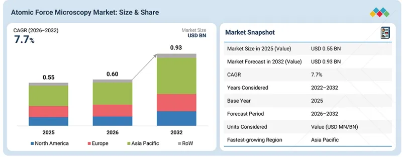
Manufacturers are increasingly developing atomic force microscope systems, specialized probes, and software to improve imaging resolution, measurement accuracy, automation, scanning capabilities, and data analysis. Advancements in automated measurements, large-sample characterization, specialized probes, and multimodal measurement techniques are further supporting market growth. The growing use of atomic force microscopes in semiconductor manufacturing, advanced materials research, chemical and polymer analysis, life sciences, and industrial quality control is creating additional opportunities for high-performance nanoscale characterization solutions.
"Research segment to account for the largest share of the atomic force microscopy market in 2032"
By grade, the research segment is expected to capture the largest market share in 2032, as atomic force microscopes are widely used by universities, research institutions, and industrial research laboratories for detailed nanoscale imaging and material characterization. These systems are used to study surface morphology, roughness, defects, thin films, nanomaterials, polymers, and biological samples across materials science and nanotechnology, chemical and polymer research, life sciences, and semiconductor research. In addition, increasing research activities in nanotechnology, advanced materials, semiconductor devices, and biological materials are augmenting the demand for high-resolution atomic force microscope systems. Advancements in imaging resolution, automated measurements, specialized probes, and multimodal characterization are further expanding the use of atomic force microscopes in research applications and supporting the growth of the research segment.
"Semiconductors & electronics segment to register the highest CAGR between 2026 and 2032"
By application, the semiconductors & electronics segment is expected to witness the highest CAGR in the atomic force microscopy market during the forecast period, driven by the increasing need for precise nanoscale surface characterization in semiconductor manufacturing and electronics research. Atomic force microscopes are used to measure surface roughness, examine wafer surfaces, identify nanoscale defects, and characterize thin films and device structures. The increasing complexity of semiconductor devices and the growing adoption of advanced materials are further increasing the need for high-resolution characterization technologies during process development, quality control, and failure analysis. In addition, advancements in automated measurements, high-resolution imaging, and specialized probes are improving the capabilities of atomic force microscopes and supporting their wider adoption across semiconductor and electronics applications.
"Asia Pacific to account for the largest share of the atomic force microscopy market in 2032"
By region, Asia Pacific is expected to hold the largest market share in 2032, supported by the strong semiconductor and electronics manufacturing base, expanding research activities, and increasing investments in nanotechnology and advanced materials. Countries such as China, Japan, South Korea, and India are increasingly adopting nanoscale characterization technologies for wafer analysis, surface characterization, thin-film measurement, and materials research. The presence of major semiconductor manufacturers, research institutions, and advanced manufacturing facilities is further driving demand for AFM systems. In addition, growing applications in materials science, nanotechnology, life sciences, chemical and polymer research, and industrial quality control are contributing to the regional market growth.
Breakdown of Primaries
A variety of executives from key organizations operating in the atomic force microscopy market were interviewed in-depth, including CEOs, marketing directors, and innovation and technology directors.
- By Company Type: Tier 1 - 40%, Tier 2 - 35%, and Tier 3 - 25%
- By Designation: C-level Executives - 48%, Directors - 33%, and Others - 19%
- By Region: North America - 35%, Europe - 18%, Asia Pacific - 40%, and RoW - 7%
Major players profiled in this report are Park Systems (South Korea), Bruker (US), Oxford Instruments (UK), Hitachi High-Tech Corporation (Japan), Semilab Inc. (US), HORIBA (Japan), Anton Paar GmbH (Austria), Nanosurf (Switzerland), NT-MDT SI (Russia), and Attocube Systems AG (Germany), among others.
These companies compete by continuously improving imaging resolution, measurement accuracy, scanning capabilities, automation, probe performance, and application-specific functionality. Strategic emphasis is placed on developing advanced atomic force microscope systems, specialized probes, automated measurement capabilities, large-sample imaging, and software solutions for applications such as semiconductor and electronics, materials science and nanotechnology, chemical and polymer research, life sciences, and industrial characterization. Market participants focus on providing high-performance atomic force microscope solutions for research institutions, semiconductor manufacturers, materials companies, and industrial users. Strong emphasis is also placed on improving surface imaging, roughness measurement, defect detection, measurement repeatability, scanning speed, and data analysis capabilities. Continued investments in research and development, advanced probe technologies, automated measurements, multimodal characterization, large-sample systems, and application-specific solutions, along with collaborations with research institutions, semiconductor manufacturers, materials companies, and industrial users, are expected to strengthen competition and support the adoption of advanced atomic force microscope solutions globally.
The study includes an in-depth competitive analysis of these key players in the atomic force microscopy market, with their company profiles, recent developments, and key market strategies.
Study Coverage
The report segments the atomic force microscopy market and forecasts its market size by offering (atomic force microscopes, probes, and software), grade (industrial and research), and application (semiconductors & electronics, materials science & nanotechnology, chemical & polymer research, life sciences, and other applications). The report also analyzes key market drivers, restraints, opportunities, and challenges influencing industry growth. It provides a detailed regional assessment across North America, Europe, Asia Pacific, and RoW, along with country-level insights for major markets. In addition, the study includes value chain analysis and competitive landscape assessment of leading players operating in the global atomic force microscopy market.
Key Benefits of Buying the Report:
- Market Dynamics: Analysis of key drivers (Need for nanoscale precision in semiconductor manufacturing, High investments in nanotechnology), restraints (Damage to samples due to contact-mode atomic force microscopy, Critical sample preparation requirements), opportunities (Increasing investments in OLED panel production globally, Expanding applications of atomic force microscopy from drug delivery to protein dynamics, Shifting application scope from basic imaging to multi-modal analysis), and challenges (High-throughput challenges due to surface coverage and speed limitations)influencing the atomic force microscopy market growth
- Product and Service Development/Innovation: Detailed insights into upcoming technologies, research and development activities, advanced measurement techniques, and new product developments in the market, including atomic force microscope systems, specialized probes, automated measurement solutions, large-sample systems, and software for imaging and data analysis
- Market Development: Comprehensive information about lucrative markets by analyzing the market across varied regions
- Market Diversification: Exhaustive information about new products/services, untapped geographies, recent developments, and investments in the market
- Competitive Assessment: In-depth assessment of the competitive landscape, market strategies, product offerings, and recent developments of leading players, such as Park Systems (South Korea), Bruker (US), Oxford Instruments (UK), Hitachi High-Tech Corporation (Japan), Semilab Inc. (US), HORIBA (Japan), Anton Paar GmbH (Austria), Nanosurf (Switzerland), NT-MDT SI (Russia), and Attocube Systems AG (Germany)
TABLE OF CONTENTS
1 INTRODUCTION
- 1.1 STUDY OBJECTIVES
- 1.2 MARKET DEFINITION
- 1.3 STUDY SCOPE
- 1.3.1 MARKETS COVERED AND REGIONAL SCOPE
- 1.3.2 YEARS CONSIDERED
- 1.3.3 INCLUSIONS AND EXCLUSIONS
- 1.4 CURRENCY CONSIDERED
- 1.5 STAKEHOLDERS
- 1.6 SUMMARY OF CHANGES
2 EXECUTIVE SUMMARY
- 2.1 MARKET HIGHLIGHTS AND KEY INSIGHTS
- 2.2 KEY MARKET PARTICIPANTS: MAPPING OF STRATEGIC DEVELOPMENTS
- 2.3 DISRUPTIVE TRENDS IN ATOMIC FORCE MICROSCOPY MARKET
- 2.4 HIGH-GROWTH SEGMENTS
- 2.5 REGIONAL SNAPSHOT: MARKET SIZE, GROWTH RATE, AND FORECAST
3 PREMIUM INSIGHTS
- 3.1 ATTRACTIVE OPPORTUNITIES FOR PLAYERS IN ATOMIC FORCE MICROSCOPY MARKET
- 3.2 ATOMIC FORCE MICROSCOPY MARKET, BY OFFERING
- 3.3 ATOMIC FORCE MICROSCOPY MARKET, BY GRADE
- 3.4 ATOMIC FORCE MICROSCOPY MARKET, BY APPLICATION
- 3.5 ATOMIC FORCE MICROSCOPY MARKET, BY GEOGRAPHY
4 MARKET OVERVIEW
- 4.1 INTRODUCTION
- 4.2 MARKET DYNAMICS
- 4.2.1 DRIVERS
- 4.2.1.1 Need for nanoscale precision in semiconductor manufacturing
- 4.2.1.2 High investments in nanotechnology
- 4.2.1.3 Expansion of atomic force microscopy applications in life sciences and healthcare sectors
- 4.2.2 RESTRAINTS
- 4.2.2.1 Damage to samples due to contact-mode atomic force microscopy
- 4.2.2.2 Critical sample preparation requirements
- 4.2.3 OPPORTUNITIES
- 4.2.3.1 Increasing investment in OLED panel production globally
- 4.2.3.2 Rising AFM adoption in drug delivery and protein analysis applications
- 4.2.3.3 Emerging applications due to technological advancements
- 4.2.4 CHALLENGES
- 4.2.4.1 High-throughput issues due to surface coverage and speed limitations
- 4.2.1 DRIVERS
- 4.3 UNMET NEEDS AND WHITE SPACES
- 4.4 INTERCONNECTED MARKETS AND CROSS-SECTOR OPPORTUNITIES
- 4.5 STRATEGIC MOVES BY TIER 1/2/3 PLAYERS
5 INDUSTRY TRENDS
- 5.1 INTRODUCTION
- 5.2 PORTER'S FIVE FORCES ANALYSIS
- 5.2.1 THREAT OF NEW ENTRANTS
- 5.2.2 THREAT OF SUBSTITUTES
- 5.2.3 BARGAINING POWER OF SUPPLIERS
- 5.2.4 BARGAINING POWER OF BUYERS
- 5.2.5 INTENSITY OF COMPETITIVE RIVALRY
- 5.3 MACROECONOMIC OUTLOOK
- 5.3.1 INTRODUCTION
- 5.3.2 GDP TRENDS AND FORECAST
- 5.3.3 TRENDS IN GLOBAL SEMICONDUCTOR & ELECTRONICS INDUSTRY
- 5.3.4 TRENDS IN GLOBAL LIFE SCIENCES & BIOTECHNOLOGY INDUSTRY
- 5.4 SUPPLY CHAIN ANALYSIS
- 5.5 ECOSYSTEM ANALYSIS
- 5.6 TRADE ANALYSIS
- 5.6.1 IMPORT SCENARIO (HS CODE 901210)
- 5.6.2 EXPORT SCENARIO (HS CODE 901210)
- 5.7 KEY CONFERENCES AND EVENTS, 2026-2027
- 5.8 TRENDS/DISRUPTIONS IMPACTING CUSTOMER BUSINESS
- 5.9 INVESTMENT AND FUNDING SCENARIO
- 5.10 CASE STUDY ANALYSIS
- 5.10.1 INSTITUTE OF PHOTONIC SCIENCES (ICFO) ADOPTS PARK SYSTEMS' FX40 AUTOMATED AFM PLATFORM TO ENABLE EFFICIENT MULTI-TECHNIQUE WORKFLOWS
- 5.10.2 BRUKER DEVELOPS LARGE-AREA AFM METROLOGY FOR PROCESS OPTIMIZATION
- 5.10.3 PUSAN NATIONAL UNIVERSITY ADOPTS PARK SYSTEMS' FX200 IR TO IMPROVE DATA INTERPRETATION
- 5.11 IMPACT OF US TARIFFS - ATOMIC FORCE MICROSCOPY MARKET
- 5.11.1 INTRODUCTION
- 5.11.2 KEY TARIFF RATES
- 5.11.3 PRICE IMPACT ANALYSIS
- 5.11.4 IMPACT ON COUNTRIES/REGIONS
- 5.11.4.1 US
- 5.11.4.2 Europe
- 5.11.4.3 Asia Pacific
- 5.11.5 IMPACT ON APPLICATIONS
6 TECHNOLOGICAL ADVANCEMENTS, AI-DRIVEN IMPACT, PATENTS, AND INNOVATIONS
- 6.1 KEY TECHNOLOGIES
- 6.1.1 CLOSED-LOOP FEEDBACK CONTROL
- 6.2 COMPLEMENTARY TECHNOLOGIES
- 6.2.1 NANOIMPRINT LITHOGRAPHY
- 6.2.2 OPTICAL INTERFEROMETRY
- 6.3 ADJACENT TECHNOLOGIES
- 6.3.1 MACHINE LEARNING
- 6.4 PATENT ANALYSIS
- 6.5 IMPACT OF AI ON ATOMIC FORCE MICROSCOPY MARKET
- 6.5.1 TOP USE CASES AND MARKET POTENTIAL
- 6.5.2 BEST PRACTICES FOLLOWED BY MANUFACTURERS/OEMS IN ATOMIC FORCE MICROSCOPY MARKET
- 6.5.3 CASE STUDIES RELATED TO AI IMPLEMENTATION IN ATOMIC FORCE MICROSCOPY MARKET
- 6.5.4 INTERCONNECTED ECOSYSTEM AND IMPACT ON MARKET PLAYERS
- 6.5.5 CLIENTS' READINESS TO ADOPT AI-INTEGRATED ATOMIC FORCE MICROSCOPES
7 REGULATORY LANDSCAPE
- 7.1 REGIONAL REGULATIONS AND COMPLIANCE
- 7.1.1 REGULATORY BODIES, GOVERNMENT AGENCIES, AND OTHER ORGANIZATIONS
- 7.1.2 STANDARDS
- 7.1.2.1 ISO 11952:2019
- 7.1.2.2 ASTM E2859-11(2023)
- 7.1.2.3 ISO 23729:2022
- 7.1.2.4 ISO 11775:2015
8 CUSTOMER LANDSCAPE AND BUYER BEHAVIOR
- 8.1 DECISION-MAKING PROCESS
- 8.2 INFLUENCE OF STAKEHOLDERS ON BUYING PROCESS AND THEIR EVALUATION CRITERIA
- 8.2.1 KEY STAKEHOLDERS IN BUYING PROCESS
- 8.2.2 BUYING CRITERIA
- 8.3 ADOPTION BARRIERS AND INTERNAL CHALLENGES
- 8.4 UNMET NEEDS OF VARIOUS APPLICATIONS
9 ATOMIC FORCE MICROSCOPY MARKET, BY OFFERING
- 9.1 INTRODUCTION
- 9.2 ATOMIC FORCE MICROSCOPES
- 9.2.1 FOCUS ON NANOSCALE SURFACE CHARACTERIZATION IN MATERIALS SCIENCE, SEMICONDUCTOR, AND LIFE SCIENCES APPLICATIONS TO SPUR DEMAND
- 9.3 PROBES
- 9.3.1 EMPHASIS ON IMPROVING MEASUREMENT ACCURACY TO ACCELERATE SEGMENTAL GROWTH
- 9.4 SOFTWARE
- 9.4.1 ABILITY TO IMPROVE MEASUREMENT CONSISTENCY AND REDUCE MANUAL EFFORT TO BOOST SEGMENTAL GROWTH
10 ATOMIC FORCE MICROSCOPY MARKET, BY GRADE
- 10.1 INTRODUCTION
- 10.2 INDUSTRIAL
- 10.2.1 GROWING NEED FOR PRECISE SEMICONDUCTOR METROLOGY AND PROCESS CONTROL TO FACILITATE SEGMENTAL GROWTH
- 10.3 RESEARCH
- 10.3.1 INCREASING INVESTMENT IN NANOTECHNOLOGY RESEARCH TO BOLSTER SEGMENTAL GROWTH
11 ATOMIC FORCE MICROSCOPY MARKET, BY APPLICATION
- 11.1 INTRODUCTION
- 11.2 SEMICONDUCTORS & ELECTRONICS
- 11.2.1 RISING MANUFACTURING COMPLEXITY TO CONTRIBUTE TO SEGMENTAL GROWTH
- 11.2.2 DATA STORAGE
- 11.2.3 3D-INTEGRATED CIRCUITS AND FIN FIELD-EFFECT TRANSISTORS
- 11.2.4 DISPLAYS
- 11.2.5 CARBON NANOTUBES
- 11.3 MATERIALS SCIENCE & NANOTECHNOLOGY
- 11.3.1 INCREASING RESEARCH AND DEMAND FOR ADVANCED MATERIALS TO FOSTER SEGMENTAL GROWTH
- 11.4 CHEMICAL & POLYMER RESEARCH
- 11.4.1 GROWING FOCUS ON IMPROVING POLYMER PERFORMANCE AND SURFACE QUALITY TO DRIVE MARKET
- 11.5 LIFE SCIENCES & BIOMEDICAL
- 11.5.1 RISING ADOPTION OF AFM TO CHARACTERIZE BIOLOGICAL SAMPLES UNDER NEAR-PHYSIOLOGICAL CONDITIONS TO DRIVE MARKET
- 11.5.2 CELL BIOLOGY
- 11.5.3 BIOTECHNOLOGY
- 11.5.4 PHARMACEUTICALS
- 11.6 OTHER APPLICATIONS
- 11.6.1 SOLAR CELLS
- 11.6.2 GEOSCIENCE
- 11.6.3 FORENSIC SCIENCE
- 11.6.4 FOOD TECHNOLOGY
12 ATOMIC FORCE MICROSCOPY MARKET, BY REGION
- 12.1 INTRODUCTION
- 12.2 NORTH AMERICA
- 12.2.1 US
- 12.2.1.1 Government's strategic push toward advanced nanotechnology to accelerate market growth
- 12.2.2 CANADA
- 12.2.2.1 Expanding federal funding for nanotechnology research centers to support market growth
- 12.2.3 MEXICO
- 12.2.3.1 Increasing focus on developing nanomaterials and advanced composites to stimulate market growth
- 12.2.1 US
- 12.3 EUROPE
- 12.3.1 GERMANY
- 12.3.1.1 Rising biotechnology and advanced materials research to create market growth opportunities
- 12.3.2 UK
- 12.3.2.1 Increasing biotechnology investments to boost market growth
- 12.3.3 FRANCE
- 12.3.3.1 Significant emphasis on sustainable manufacturing to facilitate market growth
- 12.3.4 ITALY
- 12.3.4.1 Rising demand for precision medicine, regenerative therapies, and bio-nanotechnology to create market growth opportunities
- 12.3.5 SPAIN
- 12.3.5.1 Government funding in nanotechnology, biotechnology, and materials science fields to foster market growth
- 12.3.6 NETHERLANDS
- 12.3.6.1 Public-private research collaborations to support market growth
- 12.3.7 RUSSIA
- 12.3.7.1 Investments in electronics and semiconductor research to augment market growth
- 12.3.8 SWITZERLAND
- 12.3.8.1 Strong research infrastructure and advanced materials development to fuel market growth
- 12.3.9 REST OF EUROPE
- 12.3.1 GERMANY
- 12.4 ASIA PACIFIC
- 12.4.1 CHINA
- 12.4.1.1 High-tech roadmap and semiconductor resilience to boost market growth
- 12.4.2 JAPAN
- 12.4.2.1 Ongoing R&D efforts across automotive sector to expedite market growth
- 12.4.3 SOUTH KOREA
- 12.4.3.1 Emphasis on semiconductor fabrication to facilitate market growth
- 12.4.4 INDIA
- 12.4.4.1 Increasing investment in biotech innovation to fuel market expansion
- 12.4.5 TAIWAN
- 12.4.5.1 Government funding for applied scientific development to drive market
- 12.4.6 AUSTRALIA
- 12.4.6.1 Tax credits and incentives offered to improve R&D effectiveness to stimulate market growth
- 12.4.7 SINGAPORE
- 12.4.7.1 Thriving semiconductor industry to enhance market momentum
- 12.4.8 MALAYSIA
- 12.4.8.1 Rising focus on enhancing industrial sector to support market growth
- 12.4.9 THAILAND
- 12.4.9.1 Transition toward high-value industries through Thailand 4.0 vision to expedite market growth
- 12.4.10 REST OF ASIA PACIFIC
- 12.4.1 CHINA
- 12.5 ROW
- 12.5.1 MIDDLE EAST
- 12.5.1.1 Innovation-led industrial growth to contribute to market growth
- 12.5.2 AFRICA
- 12.5.2.1 Expanding food & beverages and automotive industries to create market growth opportunities
- 12.5.3 SOUTH AMERICA
- 12.5.3.1 Collaborative research networks and R&D investments in medicine & biology field to foster market growth
- 12.5.1 MIDDLE EAST
13 COMPETITIVE LANDSCAPE
- 13.1 OVERVIEW
- 13.2 KEY PLAYER COMPETITIVE STRATEGIES/RIGHT TO WIN, 2023-2026
- 13.2.1 PRODUCT PORTFOLIO EXPANSION
- 13.2.2 REGIONAL FOOTPRINT EXPANSION
- 13.2.3 SOLUTION OFFERING EXPANSION
- 13.2.4 ORGANIC/INORGANIC STRATEGIES
- 13.3 REVENUE ANALYSIS, 2021-2025
- 13.4 MARKET SHARE ANALYSIS, 2025
- 13.5 COMPANY VALUATION AND FINANCIAL METRICS
- 13.6 BRAND COMPARISON
- 13.6.1 PARK SYSTEMS (SOUTH KOREA)
- 13.6.2 BRUKER (GERMANY)
- 13.6.3 OXFORD INSTRUMENTS (UK)
- 13.6.4 SEMILAB INC. (HUNGARY)
- 13.6.5 HITACHI HIGH-TECH CORPORATION (JAPAN)
- 13.7 COMPANY EVALUATION MATRIX: KEY PLAYERS, 2025
- 13.7.1 STARS
- 13.7.2 EMERGING LEADERS
- 13.7.3 PERVASIVE PLAYERS
- 13.7.4 PARTICIPANTS
- 13.7.5 COMPANY FOOTPRINT: KEY PLAYERS, 2025
- 13.7.5.1 Company footprint
- 13.7.5.2 Region footprint
- 13.7.5.3 Offering footprint
- 13.7.5.4 Grade footprint
- 13.7.5.5 Application footprint
- 13.8 COMPETITIVE SCENARIO
- 13.8.1 PRODUCT LAUNCHES
- 13.8.2 DEALS
14 COMPANY PROFILES
- 14.1 KEY PLAYERS
- 14.1.1 BRUKER
- 14.1.1.1 Business overview
- 14.1.1.2 Products/Solutions/Services offered
- 14.1.1.3 Recent developments
- 14.1.1.3.1 Product launches
- 14.1.1.3.2 Deals
- 14.1.1.4 MnM view
- 14.1.1.4.1 Key strengths/Right to win
- 14.1.1.4.2 Strategic choices
- 14.1.1.4.3 Weaknesses/Competitive threats
- 14.1.2 PARK SYSTEMS
- 14.1.2.1 Business overview
- 14.1.2.2 Products/Solutions/Services offered
- 14.1.2.3 Recent developments
- 14.1.2.3.1 Product launches
- 14.1.2.3.2 Deals
- 14.1.2.4 MnM view
- 14.1.2.4.1 Key strengths/Right to win
- 14.1.2.4.2 Strategic choices
- 14.1.2.4.3 Weaknesses/Competitive threats
- 14.1.3 OXFORD INSTRUMENTS
- 14.1.3.1 Business overview
- 14.1.3.2 Products/Solutions/Services offered
- 14.1.3.3 Recent developments
- 14.1.3.3.1 Product launches
- 14.1.3.3.2 Expansions
- 14.1.3.4 MnM view
- 14.1.3.4.1 Key strengths/Right to win
- 14.1.3.4.2 Strategic choices
- 14.1.3.4.3 Weaknesses/Competitive threats
- 14.1.4 SEMILAB INC.
- 14.1.4.1 Business overview
- 14.1.4.2 Products/Solutions/Services offered
- 14.1.4.3 Recent developments
- 14.1.4.3.1 Product launches
- 14.1.4.3.2 Deals
- 14.1.4.4 MnM view
- 14.1.4.4.1 Key strengths/Right to win
- 14.1.4.4.2 Strategic choices
- 14.1.4.4.3 Weaknesses/Competitive threats
- 14.1.5 HITACHI HIGH-TECH CORPORATION
- 14.1.5.1 Business overview
- 14.1.5.2 Products/Solutions/Services offered
- 14.1.5.3 MnM view
- 14.1.5.3.1 Key strengths/Right to win
- 14.1.5.3.2 Strategic choices
- 14.1.5.3.3 Weaknesses/Competitive threats
- 14.1.6 NANOSURF
- 14.1.6.1 Business overview
- 14.1.6.2 Products/Solutions/Services offered
- 14.1.6.3 Recent developments
- 14.1.6.3.1 Expansions
- 14.1.7 AFM WORKSHOP
- 14.1.7.1 Business overview
- 14.1.7.2 Products/Solutions/Services offered
- 14.1.7.3 Recent developments
- 14.1.7.3.1 Deals
- 14.1.8 ATTOCUBE SYSTEMS GMBH
- 14.1.8.1 Business overview
- 14.1.8.2 Products/Solutions/Services offered
- 14.1.9 ANTON PAAR GMBH
- 14.1.9.1 Business overview
- 14.1.9.2 Products/Solutions/Services offered
- 14.1.9.3 Recent developments
- 14.1.9.3.1 Expansions
- 14.1.10 NT-MDT SI
- 14.1.10.1 Business overview
- 14.1.10.2 Products/Solutions/Services offered
- 14.1.11 HORIBA, LTD.
- 14.1.11.1 Business overview
- 14.1.11.2 Products/solutions/services offered
- 14.1.11.3 Recent developments
- 14.1.1 BRUKER
- 14.2 OTHER PLAYERS
- 14.2.1 CSINSTRUMENTS
- 14.2.2 LABMATE SCIENTIFIC LLC
- 14.2.3 NANOMAGNETICS INSTRUMENTS
- 14.2.4 MOLECULAR VISTA
- 14.2.5 ICSPI
- 14.2.6 ANFATEC INSTRUMENTS AG
- 14.2.7 CREATEC FISCHER & CO. GMBH
- 14.2.8 A.P.E. RESEARCH
- 14.2.9 OME TECHNOLOGY CO., LTD.
- 14.2.10 DME SCANNING PROBE MICROSCOPES
- 14.2.11 GETEC MICROSCOPY GMBH
- 14.2.12 LABTRON EQUIPMENT LTD.
- 14.2.13 RHK TECHNOLOGY
- 14.2.14 MAD CITY LABS INC.
15 RESEARCH METHODOLOGY
- 15.1 RESEARCH DATA
- 15.1.1 SECONDARY DATA
- 15.1.1.1 List of key secondary sources
- 15.1.1.2 Key data from secondary sources
- 15.1.2 PRIMARY DATA
- 15.1.2.1 Breakdown of primary interviews
- 15.1.2.2 Key data from primary sources
- 15.1.2.3 Key industry insights
- 15.1.3 SECONDARY AND PRIMARY RESEARCH
- 15.1.1 SECONDARY DATA
- 15.2 MARKET SIZE ESTIMATION
- 15.2.1 BOTTOM-UP APPROACH
- 15.2.1.1 Approach to arrive at market size using bottom-up analysis (demand side)
- 15.2.2 TOP-DOWN APPROACH
- 15.2.2.1 Approach to arrive at market size using top-down analysis (supply side)
- 15.2.1 BOTTOM-UP APPROACH
- 15.3 FACTOR ANALYSIS
- 15.3.1 DEMAND-SIDE ANALYSIS
- 15.3.2 SUPPLY-SIDE ANALYSIS
- 15.4 DATA TRIANGULATION
- 15.5 RESEARCH ASSUMPTIONS
- 15.6 RISK ANALYSIS
- 15.7 RESEARCH LIMITATIONS
16 APPENDIX
- 16.1 KNOWLEDGESTORE: MARKETSANDMARKETS' SUBSCRIPTION PORTAL
- 16.2 CUSTOMIZATION OPTIONS
- 16.3 RELATED REPORTS
- 16.4 AUTHOR DETAILS
List of Tables
- TABLE 1 ATOMIC FORCE MICROSCOPY MARKET: INCLUSIONS AND EXCLUSIONS
- TABLE 2 ATOMIC FORCE MICROSCOPY MARKET: SUMMARY OF CHANGES
- TABLE 3 STRATEGIC FOCUS OF TIER 1/2/ 3 PLAYERS
- TABLE 4 IMPACT OF PORTER'S FIVE FORCES ANALYSIS
- TABLE 5 GDP PERCENTAGE CHANGE, BY KEY COUNTRY, 2021-2030
- TABLE 6 ROLE OF COMPANIES IN ATOMIC FORCE MICROSCOPY ECOSYSTEM
- TABLE 7 IMPORT DATA FOR HS CODE 901210-COMPLIANT PRODUCTS, BY COUNTRY, 2021-2025 (USD MILLION)
- TABLE 8 EXPORT DATA FOR HS CODE 901210-COMPLIANT PRODUCTS, BY COUNTRY, 2021-2025 (USD MILLION)
- TABLE 9 LIST OF KEY CONFERENCES AND EVENTS, 2026-2027
- TABLE 10 INSTITUTE OF PHOTONIC SCIENCES (ICFO) STREAMLINES AFM WORKFLOWS IN MULTI-USER RESEARCH LABORATORY
- TABLE 11 BRUKER ENABLES HIGH-THROUGHPUT, FULL-DIE NANOSCALE TOPOGRAPHY MEASUREMENT FOR SEMICONDUCTOR PROCESS CONTROL
- TABLE 12 PUSAN NATIONAL UNIVERSITY USES AFM-BASED NANO-IR TO CHARACTERIZE SEMICONDUCTOR THIN FILMS
- TABLE 13 US-ADJUSTED RECIPROCAL TARIFF RATES
- TABLE 14 EVOLUTION OF ATOMIC FORCE MICROSCOPY TECHNOLOGIES
- TABLE 15 LIST OF MAJOR PATENTS, 2023-2025
- TABLE 16 KEY USE CASES AND MARKET POTENTIAL
- TABLE 17 BEST PRACTICES ADOPTED BY MARKET PLAYERS, BY USE CASE
- TABLE 18 CASE STUDIES RELATED TO AI IMPLEMENTATION
- TABLE 19 INTERCONNECTED ECOSYSTEM AND INFLUENCE ON MARKET PLAYERS
- TABLE 20 NORTH AMERICA: LIST OF REGULATORY BODIES, GOVERNMENT AGENCIES, AND OTHER ORGANIZATIONS
- TABLE 21 EUROPE: LIST OF REGULATORY BODIES, GOVERNMENT AGENCIES, AND OTHER ORGANIZATIONS
- TABLE 22 ASIA PACIFIC: LIST OF REGULATORY BODIES, GOVERNMENT AGENCIES, AND OTHER ORGANIZATIONS
- TABLE 23 ROW: LIST OF REGULATORY BODIES, GOVERNMENT AGENCIES, AND OTHER ORGANIZATIONS
- TABLE 24 INFLUENCE OF STAKEHOLDERS ON BUYING PROCESS FOR TOP THREE APPLICATIONS (%)
- TABLE 25 KEY BUYING CRITERIA FOR TOP THREE APPLICATIONS
- TABLE 26 UNMET NEEDS, BY APPLICATION
- TABLE 27 ATOMIC FORCE MICROSCOPY MARKET, BY OFFERING, 2022-2025 (USD MILLION)
- TABLE 28 ATOMIC FORCE MICROSCOPY MARKET, BY OFFERING, 2026-2032 (USD MILLION)
- TABLE 29 FEATURES OF ATOMIC FORCE MICROSCOPY PROBES, BY TIP COATING MATERIAL
- TABLE 30 ATOMIC FORCE MICROSCOPY MARKET, BY GRADE, 2022-2025 (USD MILLION)
- TABLE 31 ATOMIC FORCE MICROSCOPY MARKET, BY GRADE, 2026-2032 (USD MILLION)
- TABLE 32 INDUSTRIAL: ATOMIC FORCE MICROSCOPY MARKET, BY APPLICATION, 2022-2025 (USD MILLION)
- TABLE 33 INDUSTRIAL: ATOMIC FORCE MICROSCOPY MARKET, BY APPLICATION, 2026-2032 (USD MILLION)
- TABLE 34 RESEARCH: ATOMIC FORCE MICROSCOPY MARKET, BY APPLICATION, 2022-2025 (USD MILLION)
- TABLE 35 RESEARCH: ATOMIC FORCE MICROSCOPY MARKET, BY APPLICATION, 2026-2032 (USD MILLION)
- TABLE 36 ATOMIC FORCE MICROSCOPY MARKET, BY APPLICATION, 2022-2025 (USD MILLION)
- TABLE 37 ATOMIC FORCE MICROSCOPY MARKET, BY APPLICATION, 2026-2032 (USD MILLION)
- TABLE 38 SEMICONDUCTORS & ELECTRONICS: ATOMIC FORCE MICROSCOPY MARKET, BY GRADE, 2022-2025 (USD MILLION)
- TABLE 39 SEMICONDUCTORS & ELECTRONICS: ATOMIC FORCE MICROSCOPY MARKET, BY GRADE, 2026-2032 (USD MILLION)
- TABLE 40 SEMICONDUCTORS & ELECTRONICS: ATOMIC FORCE MICROSCOPY MARKET, BY REGION, 2022-2025 (USD MILLION)
- TABLE 41 SEMICONDUCTORS & ELECTRONICS: ATOMIC FORCE MICROSCOPY MARKET, BY REGION, 2026-2032 (USD MILLION)
- TABLE 42 SEMICONDUCTORS & ELECTRONICS: ATOMIC FORCE MICROSCOPY MARKET IN NORTH AMERICA, BY COUNTRY, 2022-2025 (USD MILLION)
- TABLE 43 SEMICONDUCTORS & ELECTRONICS: ATOMIC FORCE MICROSCOPY MARKET IN NORTH AMERICA, BY COUNTRY, 2026-2032 (USD MILLION)
- TABLE 44 SEMICONDUCTORS & ELECTRONICS: ATOMIC FORCE MICROSCOPY MARKET IN EUROPE, BY COUNTRY, 2022-2025 (USD MILLION)
- TABLE 45 SEMICONDUCTORS & ELECTRONICS: ATOMIC FORCE MICROSCOPY MARKET IN EUROPE, BY COUNTRY, 2026-2032 (USD MILLION)
- TABLE 46 SEMICONDUCTORS & ELECTRONICS: ATOMIC FORCE MICROSCOPY MARKET IN ASIA PACIFIC, BY COUNTRY, 2022-2025 (USD MILLION)
- TABLE 47 SEMICONDUCTORS & ELECTRONICS: ATOMIC FORCE MICROSCOPY MARKET IN ASIA PACIFIC, BY COUNTRY, 2026-2032 (USD MILLION)
- TABLE 48 SEMICONDUCTORS & ELECTRONICS: ATOMIC FORCE MICROSCOPY MARKET IN ROW, BY REGION, 2022-2025 (USD MILLION)
- TABLE 49 SEMICONDUCTORS & ELECTRONICS: ATOMIC FORCE MICROSCOPY MARKET IN ROW, BY REGION, 2026-2032 (USD MILLION)
- TABLE 50 MATERIALS SCIENCE & NANOTECHNOLOGY: ATOMIC FORCE MICROSCOPY MARKET, BY GRADE, 2022-2025 (USD MILLION)
- TABLE 51 MATERIALS SCIENCE & NANOTECHNOLOGY: ATOMIC FORCE MICROSCOPY MARKET, BY GRADE, 2026-2032 (USD MILLION)
- TABLE 52 MATERIALS SCIENCE & NANOTECHNOLOGY: ATOMIC FORCE MICROSCOPY MARKET, BY REGION, 2022-2025 (USD MILLION)
- TABLE 53 MATERIALS SCIENCE & NANOTECHNOLOGY: ATOMIC FORCE MICROSCOPY MARKET, BY REGION, 2026-2032 (USD MILLION)
- TABLE 54 MATERIALS SCIENCE & NANOTECHNOLOGY: ATOMIC FORCE MICROSCOPY MARKET IN NORTH AMERICA, BY COUNTRY, 2022-2025 (USD MILLION)
- TABLE 55 MATERIALS SCIENCE & NANOTECHNOLOGY: ATOMIC FORCE MICROSCOPY MARKET IN NORTH AMERICA, BY COUNTRY, 2026-2032 (USD MILLION)
- TABLE 56 MATERIALS SCIENCE & NANOTECHNOLOGY: ATOMIC FORCE MICROSCOPY MARKET IN EUROPE, BY COUNTRY, 2022-2025 (USD MILLION)
- TABLE 57 MATERIALS SCIENCE & NANOTECHNOLOGY: ATOMIC FORCE MICROSCOPY MARKET IN EUROPE, BY COUNTRY, 2026-2032 (USD MILLION)
- TABLE 58 MATERIALS SCIENCE & NANOTECHNOLOGY: ATOMIC FORCE MICROSCOPY MARKET IN ASIA PACIFIC, BY COUNTRY, 2022-2025 (USD MILLION)
- TABLE 59 MATERIALS SCIENCE & NANOTECHNOLOGY: ATOMIC FORCE MICROSCOPY MARKET IN ASIA PACIFIC, BY COUNTRY, 2026-2032 (USD MILLION)
- TABLE 60 MATERIALS SCIENCE & NANOTECHNOLOGY: ATOMIC FORCE MICROSCOPY MARKET IN ROW, BY REGION, 2022-2025 (USD MILLION)
- TABLE 61 MATERIALS SCIENCE & NANOTECHNOLOGY: ATOMIC FORCE MICROSCOPY MARKET IN ROW, BY REGION, 2026-2032 (USD MILLION)
- TABLE 62 CHEMICAL & POLYMER RESEARCH: ATOMIC FORCE MICROSCOPY MARKET, BY GRADE, 2022-2025 (USD MILLION)
- TABLE 63 CHEMICAL & POLYMER RESEARCH: ATOMIC FORCE MICROSCOPY MARKET, BY GRADE, 2026-2032 (USD MILLION)
- TABLE 64 CHEMICAL & POLYMER RESEARCH: ATOMIC FORCE MICROSCOPY MARKET, BY REGION, 2022-2025 (USD MILLION)
- TABLE 65 CHEMICAL & POLYMER RESEARCH: ATOMIC FORCE MICROSCOPY MARKET, BY REGION, 2026-2032 (USD MILLION)
- TABLE 66 CHEMICAL & POLYMER RESEARCH: ATOMIC FORCE MICROSCOPY MARKET IN NORTH AMERICA, BY COUNTRY, 2022-2025 (USD MILLION)
- TABLE 67 CHEMICAL & POLYMER RESEARCH: ATOMIC FORCE MICROSCOPY MARKET IN NORTH AMERICA, BY COUNTRY, 2026-2032 (USD MILLION)
- TABLE 68 CHEMICAL & POLYMER RESEARCH: ATOMIC FORCE MICROSCOPY MARKET IN EUROPE, BY COUNTRY, 2022-2025 (USD MILLION)
- TABLE 69 CHEMICAL & POLYMER RESEARCH: ATOMIC FORCE MICROSCOPY MARKET IN EUROPE, BY COUNTRY, 2026-2032 (USD MILLION)
- TABLE 70 CHEMICAL & POLYMER RESEARCH: ATOMIC FORCE MICROSCOPY MARKET IN ASIA PACIFIC, BY COUNTRY, 2022-2025 (USD MILLION)
- TABLE 71 CHEMICAL & POLYMER RESEARCH: ATOMIC FORCE MICROSCOPY MARKET IN ASIA PACIFIC, BY COUNTRY, 2026-2032 (USD MILLION)
- TABLE 72 CHEMICAL & POLYMER RESEARCH: ATOMIC FORCE MICROSCOPY MARKET IN ROW, BY REGION, 2022-2025 (USD MILLION)
- TABLE 73 CHEMICAL & POLYMER RESEARCH: ATOMIC FORCE MICROSCOPY MARKET IN ROW, BY REGION, 2026-2032 (USD MILLION)
- TABLE 74 LIFE SCIENCES & BIOMEDICAL: ATOMIC FORCE MICROSCOPY MARKET, BY GRADE, 2022-2025 (USD MILLION)
- TABLE 75 LIFE SCIENCES & BIOMEDICAL: ATOMIC FORCE MICROSCOPY MARKET, BY GRADE, 2026-2032 (USD MILLION)
- TABLE 76 LIFE SCIENCES & BIOMEDICAL: ATOMIC FORCE MICROSCOPY MARKET, BY REGION, 2022-2025 (USD MILLION)
- TABLE 77 LIFE SCIENCES & BIOMEDICAL: ATOMIC FORCE MICROSCOPY MARKET, BY REGION, 2026-2032 (USD MILLION)
- TABLE 78 LIFE SCIENCES & BIOMEDICAL: ATOMIC FORCE MICROSCOPY MARKET IN NORTH AMERICA, BY COUNTRY, 2022-2025 (USD MILLION)
- TABLE 79 LIFE SCIENCES & BIOMEDICAL: ATOMIC FORCE MICROSCOPY MARKET IN NORTH AMERICA, BY COUNTRY, 2026-2032 (USD MILLION)
- TABLE 80 LIFE SCIENCES & BIOMEDICAL: ATOMIC FORCE MICROSCOPY MARKET IN EUROPE, BY COUNTRY, 2022-2025 (USD MILLION)
- TABLE 81 LIFE SCIENCES & BIOMEDICAL: ATOMIC FORCE MICROSCOPY MARKET IN EUROPE, BY COUNTRY, 2026-2032 (USD MILLION)
- TABLE 82 LIFE SCIENCES & BIOMEDICAL: ATOMIC FORCE MICROSCOPY MARKET IN ASIA PACIFIC, BY COUNTRY, 2022-2025 (USD MILLION)
- TABLE 83 LIFE SCIENCES & BIOMEDICAL: ATOMIC FORCE MICROSCOPY MARKET IN ASIA PACIFIC, BY COUNTRY, 2026-2032 (USD MILLION)
- TABLE 84 LIFE SCIENCES & BIOMEDICAL: ATOMIC FORCE MICROSCOPY MARKET IN ROW, BY REGION, 2022-2025 (USD MILLION)
- TABLE 85 LIFE SCIENCES & BIOMEDICAL: ATOMIC FORCE MICROSCOPY MARKET IN ROW, BY REGION, 2026-2032 (USD MILLION)
- TABLE 86 OTHER APPLICATIONS: ATOMIC FORCE MICROSCOPY MARKET, BY GRADE, 2022-2025 (USD MILLION)
- TABLE 87 OTHER APPLICATIONS: ATOMIC FORCE MICROSCOPY MARKET, BY GRADE, 2026-2032 (USD MILLION)
- TABLE 88 OTHER APPLICATIONS: ATOMIC FORCE MICROSCOPY MARKET, BY REGION, 2022-2025 (USD MILLION)
- TABLE 89 OTHER APPLICATIONS: ATOMIC FORCE MICROSCOPY MARKET, BY REGION, 2026-2032 (USD MILLION)
- TABLE 90 OTHER APPLICATIONS: ATOMIC FORCE MICROSCOPY MARKET IN NORTH AMERICA, BY COUNTRY, 2022-2025 (USD MILLION)
- TABLE 91 OTHER APPLICATIONS: ATOMIC FORCE MICROSCOPY MARKET IN NORTH AMERICA, BY COUNTRY, 2026-2032 (USD MILLION)
- TABLE 92 OTHER APPLICATIONS: ATOMIC FORCE MICROSCOPY MARKET IN EUROPE, BY COUNTRY, 2022-2025 (USD MILLION)
- TABLE 93 OTHER APPLICATIONS: ATOMIC FORCE MICROSCOPY MARKET IN EUROPE, BY COUNTRY, 2026-2032 (USD MILLION)
- TABLE 94 OTHER APPLICATIONS: ATOMIC FORCE MICROSCOPY MARKET IN ASIA PACIFIC, BY COUNTRY, 2022-2025 (USD MILLION)
- TABLE 95 OTHER APPLICATIONS: ATOMIC FORCE MICROSCOPY MARKET IN ASIA PACIFIC, BY COUNTRY, 2026-2032 (USD MILLION)
- TABLE 96 OTHER APPLICATIONS: ATOMIC FORCE MICROSCOPY MARKET IN ROW, BY REGION, 2022-2025 (USD MILLION)
- TABLE 97 OTHER APPLICATIONS: ATOMIC FORCE MICROSCOPY MARKET IN ROW, BY REGION, 2026-2032 (USD MILLION)
- TABLE 98 ATOMIC FORCE MICROSCOPY MARKET, BY REGION, 2022-2025 (USD MILLION)
- TABLE 99 ATOMIC FORCE MICROSCOPY MARKET, BY REGION, 2026-2032 (USD MILLION)
- TABLE 100 NORTH AMERICA: ATOMIC FORCE MICROSCOPY MARKET, BY APPLICATION, 2022-2025 (USD MILLION)
- TABLE 101 NORTH AMERICA: ATOMIC FORCE MICROSCOPY MARKET, BY APPLICATION, 2026-2032 (USD MILLION)
- TABLE 102 NORTH AMERICA: ATOMIC FORCE MICROSCOPY MARKET, BY COUNTRY, 2022-2025 (USD MILLION)
- TABLE 103 NORTH AMERICA: ATOMIC FORCE MICROSCOPY MARKET, BY COUNTRY, 2026-2032 (USD MILLION)
- TABLE 104 US: ATOMIC FORCE MICROSCOPY MARKET, BY APPLICATION, 2022-2025 (USD MILLION)
- TABLE 105 US: ATOMIC FORCE MICROSCOPY MARKET, BY APPLICATION, 2026-2032 (USD MILLION)
- TABLE 106 CANADA: ATOMIC FORCE MICROSCOPY MARKET, BY APPLICATION, 2022-2025 (USD MILLION)
- TABLE 107 CANADA: ATOMIC FORCE MICROSCOPY MARKET, BY APPLICATION, 2026-2032 (USD MILLION)
- TABLE 108 MEXICO: ATOMIC FORCE MICROSCOPY MARKET, BY APPLICATION, 2022-2025 (USD MILLION)
- TABLE 109 MEXICO: ATOMIC FORCE MICROSCOPY MARKET, BY APPLICATION, 2026-2032 (USD MILLION)
- TABLE 110 EUROPE: ATOMIC FORCE MICROSCOPY MARKET, BY APPLICATION, 2022-2025 (USD MILLION)
- TABLE 111 EUROPE: ATOMIC FORCE MICROSCOPY MARKET, BY APPLICATION, 2026-2032 (USD MILLION)
- TABLE 112 EUROPE: ATOMIC FORCE MICROSCOPY MARKET, BY COUNTRY, 2022-2025 (USD MILLION)
- TABLE 113 EUROPE: ATOMIC FORCE MICROSCOPY MARKET, BY COUNTRY, 2026-2032 (USD MILLION)
- TABLE 114 GERMANY: ATOMIC FORCE MICROSCOPY MARKET, BY APPLICATION, 2022-2025 (USD MILLION)
- TABLE 115 GERMANY: ATOMIC FORCE MICROSCOPY MARKET, BY APPLICATION, 2026-2032 (USD MILLION)
- TABLE 116 UK: ATOMIC FORCE MICROSCOPY MARKET, BY APPLICATION, 2022-2025 (USD MILLION)
- TABLE 117 UK: ATOMIC FORCE MICROSCOPY MARKET, BY APPLICATION, 2026-2032 (USD MILLION)
- TABLE 118 FRANCE: ATOMIC FORCE MICROSCOPY MARKET, BY APPLICATION, 2022-2025 (USD MILLION)
- TABLE 119 FRANCE: ATOMIC FORCE MICROSCOPY MARKET, BY APPLICATION, 2026-2032 (USD MILLION)
- TABLE 120 ITALY: ATOMIC FORCE MICROSCOPY MARKET, BY APPLICATION, 2022-2025 (USD MILLION)
- TABLE 121 ITALY: ATOMIC FORCE MICROSCOPY MARKET, BY APPLICATION, 2026-2032 (USD MILLION)
- TABLE 122 SPAIN: ATOMIC FORCE MICROSCOPY MARKET, BY APPLICATION, 2022-2025 (USD MILLION)
- TABLE 123 SPAIN: ATOMIC FORCE MICROSCOPY MARKET, BY APPLICATION, 2026-2032 (USD MILLION)
- TABLE 124 NETHERLANDS: ATOMIC FORCE MICROSCOPY MARKET, BY APPLICATION, 2022-2025 (USD MILLION)
- TABLE 125 NETHERLANDS: ATOMIC FORCE MICROSCOPY MARKET, BY APPLICATION, 2026-2032 (USD MILLION)
- TABLE 126 RUSSIA: ATOMIC FORCE MICROSCOPY MARKET, BY APPLICATION, 2022-2025 (USD MILLION)
- TABLE 127 RUSSIA: ATOMIC FORCE MICROSCOPY MARKET, BY APPLICATION, 2026-2032 (USD MILLION)
- TABLE 128 SWITZERLAND: ATOMIC FORCE MICROSCOPY MARKET, BY APPLICATION, 2022-2025 (USD MILLION)
- TABLE 129 SWITZERLAND: ATOMIC FORCE MICROSCOPY MARKET, BY APPLICATION, 2026-2032 (USD MILLION)
- TABLE 130 REST OF EUROPE: ATOMIC FORCE MICROSCOPY MARKET, BY APPLICATION, 2022-2025 (USD MILLION)
- TABLE 131 REST OF EUROPE: ATOMIC FORCE MICROSCOPY MARKET, BY APPLICATION, 2026-2032 (USD MILLION)
- TABLE 132 ASIA PACIFIC: ATOMIC FORCE MICROSCOPY MARKET, BY APPLICATION, 2022-2025 (USD MILLION)
- TABLE 133 ASIA PACIFIC: ATOMIC FORCE MICROSCOPY MARKET, BY APPLICATION, 2026-2032 (USD MILLION)
- TABLE 134 ASIA PACIFIC: ATOMIC FORCE MICROSCOPY MARKET, BY COUNTRY, 2022-2025 (USD MILLION)
- TABLE 135 ASIA PACIFIC: ATOMIC FORCE MICROSCOPY MARKET, BY COUNTRY, 2026-2032 (USD MILLION)
- TABLE 136 CHINA: ATOMIC FORCE MICROSCOPY MARKET, BY APPLICATION, 2022-2025 (USD MILLION)
- TABLE 137 CHINA: ATOMIC FORCE MICROSCOPY MARKET, BY APPLICATION, 2026-2032 (USD MILLION)
- TABLE 138 JAPAN: ATOMIC FORCE MICROSCOPY MARKET, BY APPLICATION, 2022-2025 (USD MILLION)
- TABLE 139 JAPAN: ATOMIC FORCE MICROSCOPY MARKET, BY APPLICATION, 2026-2032 (USD MILLION)
- TABLE 140 SOUTH KOREA: ATOMIC FORCE MICROSCOPY MARKET, BY APPLICATION, 2022-2025 (USD MILLION)
- TABLE 141 SOUTH KOREA: ATOMIC FORCE MICROSCOPY MARKET, BY APPLICATION, 2026-2032 (USD MILLION)
- TABLE 142 INDIA: ATOMIC FORCE MICROSCOPY MARKET, BY APPLICATION, 2022-2025 (USD MILLION)
- TABLE 143 INDIA: ATOMIC FORCE MICROSCOPY MARKET, BY APPLICATION, 2026-2032 (USD MILLION)
- TABLE 144 TAIWAN: ATOMIC FORCE MICROSCOPY MARKET, BY APPLICATION, 2022-2025 (USD MILLION)
- TABLE 145 TAIWAN: ATOMIC FORCE MICROSCOPY MARKET, BY APPLICATION, 2026-2032 (USD MILLION)
- TABLE 146 AUSTRALIA: ATOMIC FORCE MICROSCOPY MARKET, BY APPLICATION, 2022-2025 (USD MILLION)
- TABLE 147 AUSTRALIA: ATOMIC FORCE MICROSCOPY MARKET, BY APPLICATION, 2026-2032 (USD MILLION)
- TABLE 148 SINGAPORE: ATOMIC FORCE MICROSCOPY MARKET, BY APPLICATION, 2022-2025 (USD MILLION)
- TABLE 149 SINGAPORE: ATOMIC FORCE MICROSCOPY MARKET, BY APPLICATION, 2026-2032 (USD MILLION)
- TABLE 150 MALAYSIA: ATOMIC FORCE MICROSCOPY MARKET, BY APPLICATION, 2022-2025 (USD MILLION)
- TABLE 151 MALAYSIA: ATOMIC FORCE MICROSCOPY MARKET, BY APPLICATION, 2026-2032 (USD MILLION)
- TABLE 152 THAILAND: ATOMIC FORCE MICROSCOPY MARKET, BY APPLICATION, 2022-2025 (USD MILLION)
- TABLE 153 THAILAND: ATOMIC FORCE MICROSCOPY MARKET, BY APPLICATION, 2026-2032 (USD MILLION)
- TABLE 154 REST OF ASIA PACIFIC: ATOMIC FORCE MICROSCOPY MARKET, BY APPLICATION, 2022-2025 (USD MILLION)
- TABLE 155 REST OF ASIA PACIFIC: ATOMIC FORCE MICROSCOPY MARKET, BY APPLICATION, 2026-2032 (USD MILLION)
- TABLE 156 ROW: ATOMIC FORCE MICROSCOPY MARKET, BY APPLICATION, 2022-2025 (USD MILLION)
- TABLE 157 ROW: ATOMIC FORCE MICROSCOPY MARKET, BY APPLICATION, 2026-2032 (USD MILLION)
- TABLE 158 ROW: ATOMIC FORCE MICROSCOPY MARKET, BY REGION, 2022-2025 (USD MILLION)
- TABLE 159 ROW: ATOMIC FORCE MICROSCOPY MARKET, BY REGION, 2026-2032 (USD MILLION)
- TABLE 160 MIDDLE EAST: ATOMIC FORCE MICROSCOPY MARKET, BY APPLICATION, 2022-2025 (USD MILLION)
- TABLE 161 MIDDLE EAST: ATOMIC FORCE MICROSCOPY MARKET, BY APPLICATION, 2026-2032 (USD MILLION)
- TABLE 162 AFRICA: ATOMIC FORCE MICROSCOPY MARKET, BY APPLICATION, 2022-2025 (USD MILLION)
- TABLE 163 AFRICA: ATOMIC FORCE MICROSCOPY MARKET, BY APPLICATION, 2026-2032 (USD MILLION)
- TABLE 164 SOUTH AMERICA: ATOMIC FORCE MICROSCOPY MARKET, BY APPLICATION, 2022-2025 (USD MILLION)
- TABLE 165 SOUTH AMERICA: ATOMIC FORCE MICROSCOPY MARKET, BY APPLICATION, 2026-2032 (USD MILLION)
- TABLE 166 ATOMIC FORCE MICROSCOPY MARKET: OVERVIEW OF STRATEGIES ADOPTED BY KEY PLAYERS, JANUARY 2023-AUGUST 2026
- TABLE 167 ATOMIC FORCE MICROSCOPY MARKET: DEGREE OF COMPETITION, 2025
- TABLE 168 ATOMIC FORCE MICROSCOPY MARKET: REGION FOOTPRINT
- TABLE 169 ATOMIC FORCE MICROSCOPY MARKET: OFFERING FOOTPRINT
- TABLE 170 ATOMIC FORCE MICROSCOPY MARKET: GRADE FOOTPRINT
- TABLE 171 ATOMIC FORCE MICROSCOPY MARKET: APPLICATION FOOTPRINT
- TABLE 172 ATOMIC FORCE MICROSCOPY MARKET: PRODUCT LAUNCHES, JANUARY 2023-AUGUST 2026
- TABLE 173 ATOMIC FORCE MICROSCOPY MARKET: DEALS, JANUARY 2023-AUGUST 2026
- TABLE 174 BRUKER: COMPANY OVERVIEW
- TABLE 175 BRUKER: PRODUCTS/SOLUTIONS/SERVICES OFFERED
- TABLE 176 BRUKER: PRODUCT LAUNCHES
- TABLE 177 BRUKER: DEALS
- TABLE 178 PARK SYSTEMS: COMPANY OVERVIEW
- TABLE 179 PARK SYSTEMS: PRODUCTS/SOLUTIONS/SERVICES OFFERED
- TABLE 180 PARK SYSTEMS: PRODUCT LAUNCHES
- TABLE 181 PARKER SYSTEMS: DEALS
- TABLE 182 OXFORD INSTRUMENTS: COMPANY OVERVIEW
- TABLE 183 OXFORD INSTRUMENTS: PRODUCTS/SOLUTIONS/SERVICES OFFERED
- TABLE 184 OXFORD INSTRUMENTS: PRODUCT LAUNCHES
- TABLE 185 OXFORD INSTRUMENTS: EXPANSION
- TABLE 186 SEMILAB INC.: COMPANY OVERVIEW
- TABLE 187 SEMILAB INC.: PRODUCTS/SOLUTIONS/SERVICES OFFERED
- TABLE 188 SEMILAB INC.: PRODUCT LAUNCHES
- TABLE 189 SEMILAB INC.: DEALS
- TABLE 190 HITACHI HIGH-TECH CORPORATION: COMPANY OVERVIEW
- TABLE 191 HITACHI HIGH-TECH CORPORATION: PRODUCTS/SOLUTIONS/SERVICES OFFERED
- TABLE 192 HITACHI HIGH-TECH CORPORATION: OTHER DEVOLPMENTS
- TABLE 193 NANOSURF: COMPANY OVERVIEW
- TABLE 194 NANOSURF: PRODUCTS/SOLUTIONS/SERVICES OFFERED
- TABLE 195 NANOSURF: EXPANSION
- TABLE 196 AFM WORKSHOP: COMPANY OVERVIEW
- TABLE 197 AFM WORKSHOP: PRODUCTS/SOLUTIONS/SERVICES OFFERED
- TABLE 198 AFM WORKSHOP: DEALS
- TABLE 199 ATTOCUBE SYSTEMS GMBH: COMPANY OVERVIEW
- TABLE 200 ATTOCUBE SYSTEMS GMBH: PRODUCTS/SOLUTIONS/SERVICES OFFERED
- TABLE 201 ANTON PAAR GMBH: COMPANY OVERVIEW
- TABLE 202 ANTON PAAR GMBH: PRODUCTS/SOLUTIONS/SERVICES OFFERED
- TABLE 203 ANTON PAAR GMBH: EXPANSIONS
- TABLE 204 NT-MDT SI: COMPANY OVERVIEW
- TABLE 205 NT-MDT SI: PRODUCTS/SOLUTIONS/SERVICES OFFERED
- TABLE 206 HORIBA, LTD.: COMPANY OVERVIEW
- TABLE 207 HORIBA, LTD.: PRODUCTS/SOLUTIONS/SERVICES OFFERED
- TABLE 208 HORIBA, LTD.: EXPANSIONS
- TABLE 209 CSINSTRUMENTS: COMPANY OVERVIEW
- TABLE 210 LABMATE SCIENTIFIC LLC: COMPANY OVERVIEW
- TABLE 211 NANOMAGNETICS INSTRUMENTS: COMPANY OVERVIEW
- TABLE 212 MOLECULAR VISTA: COMPANY OVERVIEW
- TABLE 213 ICSPI: COMPANY OVERVIEW
- TABLE 214 ANFATEC INSTRUMENTS AG: COMPANY OVERVIEW
- TABLE 215 CREATEC FISCHER & CO. GMBH: COMPANY OVERVIEW
- TABLE 216 A.P.E. RESEARCH: COMPANY OVERVIEW
- TABLE 217 OME TECHNOLOGY CO., LTD.: COMPANY OVERVIEW
- TABLE 218 DME SCANNING PROBE MICROSCOPES: COMPANY OVERVIEW
- TABLE 219 GETEC MICROSCOPY GMBH: COMPANY OVERVIEW
- TABLE 220 LABTRON EQUIPMENT LTD.: COMPANY OVERVIEW
- TABLE 221 RHK TECHNOLOGY: COMPANY OVERVIEW
- TABLE 222 MAD CITY LABS INC.: COMPANY OVERVIEW
- TABLE 223 ATOMIC FORCE MICROSCOPY MARKET: RISK ANALYSIS
List of Figures
- FIGURE 1 ATOMIC FORCE MICROSCOPY MARKET SEGMENTATION AND REGIONAL SCOPE
- FIGURE 2 ATOMIC FORCE MICROSCOPY MARKET SCENARIO
- FIGURE 3 GLOBAL ATOMIC FORCE MICROSCOPY MARKET SIZE, 2022-2032
- FIGURE 4 MAJOR STRATEGIES ADOPTED BY KEY PLAYERS IN ATOMIC FORCE MICROSCOPY MARKET, JANUARY 2023-AUGUST 2026
- FIGURE 5 DISRUPTIONS INFLUENCING GROWTH OF ATOMIC FORCE MICROSCOPY MARKET
- FIGURE 6 HIGH-GROWTH SEGMENTS IN ATOMIC FORCE MICROSCOPY MARKET, 2026-2032
- FIGURE 7 ASIA PACIFIC TO REGISTER HIGHEST CAGR IN ATOMIC FORCE MICROSCOPY MARKET DURING FORECAST PERIOD
- FIGURE 8 RAPID EXPANSION OF SEMICONDUCTOR FABRICATION INFRASTRUCTURE AND INVESTMENT IN NANOTECHNOLOGY RESEARCH TO DRIVE MARKET
- FIGURE 9 ATOMIC FORCE MICROSCOPES SEGMENT TO HOLD LARGEST MARKET SHARE IN 2026 AND 2032
- FIGURE 10 RESEARCH SEGMENT TO CAPTURE LARGER MARKET SHARE IN 2026 AND 2032
- FIGURE 11 SEMICONDUCTORS & ELECTRONICS SEGMENT TO ACCOUNT FOR LARGEST MARKET SHARE IN 2032
- FIGURE 12 INDIA TO EXHIBIT HIGHEST CAGR IN GLOBAL ATOMIC FORCE MICROSCOPY MARKET DURING FORECAST PERIOD
- FIGURE 13 DRIVERS, RESTRAINTS, OPPORTUNITIES, AND CHALLENGES
- FIGURE 14 IMPACT ANALYSIS: DRIVERS
- FIGURE 15 IMPACT ANALYSIS: RESTRAINTS
- FIGURE 16 IMPACT ANALYSIS: OPPORTUNITIES
- FIGURE 17 IMPACT ANALYSIS: CHALLENGES
- FIGURE 18 PORTER'S FIVE FORCES ANALYSIS
- FIGURE 19 ATOMIC FORCE MICROSCOPY SUPPLY CHAIN ANALYSIS
- FIGURE 20 ATOMIC FORCE MICROSCOPY ECOSYSTEM ANALYSIS
- FIGURE 21 IMPORT DATA FOR HS CODE 901210-COMPLIANT PRODUCTS FOR TOP FIVE COUNTRIES, 2021-2025
- FIGURE 22 EXPORT DATA FOR HS CODE 901210-COMPLIANT PRODUCTS FOR TOP FIVE COUNTRIES, 2021-2025
- FIGURE 23 TRENDS/DISRUPTIONS INFLUENCING CUSTOMER BUSINESS
- FIGURE 24 INVESTMENT AND FUNDING SCENARIO, 2022-2025
- FIGURE 25 PATENTS APPLIED AND GRANTED, 2016-2025
- FIGURE 26 DECISION-MAKING FACTORS IN ATOMIC FORCE MICROSCOPY MARKET
- FIGURE 27 INFLUENCE OF STAKEHOLDERS ON BUYING PROCESS FOR TOP THREE APPLICATIONS
- FIGURE 28 KEY BUYING CRITERIA FOR TOP THREE APPLICATIONS
- FIGURE 29 AFM ADOPTION BARRIERS AND INTERNAL CHALLENGES
- FIGURE 30 ATOMIC FORCE MICROSCOPES SEGMENT TO CAPTURE MAJORITY OF MARKET SHARE IN 2026 AND 2032
- FIGURE 31 ATOMIC FORCE MICROSCOPY MARKET, BY GRADE
- FIGURE 32 RESEARCH SEGMENT TO HOLD LARGER MARKET SHARE IN 2026 AND 2032
- FIGURE 33 ATOMIC FORCE MICROSCOPY MARKET, BY APPLICATION
- FIGURE 34 SEMICONDUCTOR & ELECTRONICS SEGMENT TO DOMINATE ATOMIC FORCE MICROSCOPY MARKET DURING FORECAST PERIOD
- FIGURE 35 ASIA PACIFIC TO EXHIBIT HIGHEST CAGR IN ATOMIC FORCE MICROSCOPY MARKET DURING FORECAST PERIOD
- FIGURE 36 NORTH AMERICA: ATOMIC FORCE MICROSCOPY MARKET SNAPSHOT
- FIGURE 37 EUROPE: ATOMIC FORCE MICROSCOPY MARKET SNAPSHOT
- FIGURE 38 ASIA PACIFIC: ATOMIC FORCE MICROSCOPY MARKET SNAPSHOT
- FIGURE 39 ATOMIC FORCE MICROSCOPY MARKET: REVENUE ANALYSIS OF TOP TWO PLAYERS, 2021-2025
- FIGURE 40 MARKET SHARE ANALYSIS OF KEY PLAYERS OFFERING ATOMIC FORCE MICROSCOPY SOLUTIONS, 2025
- FIGURE 41 COMPANY VALUATION
- FIGURE 42 FINANCIAL METRICS (EV/EBITDA)
- FIGURE 43 BRAND COMPARATIVE ANALYSIS
- FIGURE 44 ATOMIC FORCE MICROSCOPY MARKET: COMPANY EVALUATION MATRIX (KEY PLAYERS), 2025
- FIGURE 45 ATOMIC FORCE MICROSCOPY MARKET: COMPANY FOOTPRINT
- FIGURE 46 BRUKER: COMPANY SNAPSHOT
- FIGURE 47 PARK SYSTEMS: COMPANY SNAPSHOT
- FIGURE 48 OXFORD INSTRUMENTS: COMPANY SNAPSHOT
- FIGURE 49 HITACHI HIGH-TECH CORPORATION: COMPANY SNAPSHOT
- FIGURE 50 HORIBA, LTD.: COMPANY SNAPSHOT
- FIGURE 51 ATOMIC FORCE MICROSCOPY MARKET: RESEARCH DESIGN
- FIGURE 52 BREAKDOWN OF PRIMARY INTERVIEWS, BY COMPANY TYPE, DESIGNATION, AND REGION
- FIGURE 53 CORE FINDINGS FROM INDUSTRY EXPERTS
- FIGURE 54 ATOMIC FORCE MICROSCOPY MARKET: RESEARCH APPROACH
- FIGURE 55 ATOMIC FORCE MICROSCOPY MARKET: BOTTOM-UP APPROACH
- FIGURE 56 ATOMIC FORCE MICROSCOPY MARKET: TOP-DOWN APPROACH
- FIGURE 57 ATOMIC FORCE MICROSCOPY MARKET SIZE ESTIMATION METHODOLOGY (SUPPLY SIDE)
- FIGURE 58 ATOMIC FORCE MICROSCOPY MARKET: DATA TRIANGULATION
- FIGURE 59 ATOMIC FORCE MICROSCOPY MARKET: RESEARCH ASSUMPTIONS

