
PUBLISHER: Mordor Intelligence | PRODUCT CODE: 1849988

PUBLISHER: Mordor Intelligence | PRODUCT CODE: 1849988
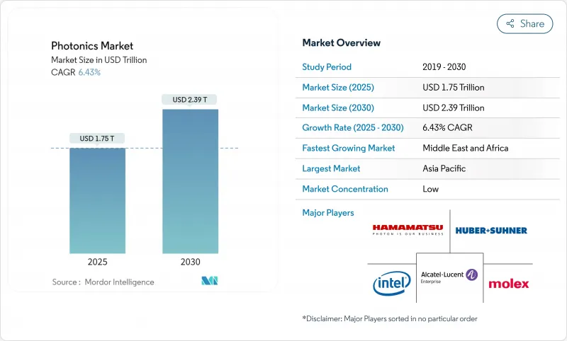
Photonics - Market Share Analysis, Industry Trends & Statistics, Growth Forecasts (2025 - 2030)
The photonics market is valued at USD 1.75 trillion in 2025 and is set to advance to USD 2.39 trillion by 2030 at a 6.43% CAGR.
Expansion rests on the rising deployment of high-speed optical links inside data centers, growing LiDAR penetration in vehicles and sustained demand for energy-efficient LED lighting. Regional supply-chain programs, such as India's PLI scheme and the EU Chips Act, are accelerating new fab construction, while corporate funding rounds for silicon-photonics start-ups signal confidence in chip-to-chip optical interconnects. Automotive OEMs are standardizing LiDAR as an ADAS staple, stimulating volume growth and cost declines. At the same time, GaN and micro-LED capacity ramp-ups underline the shift toward materials and devices that lower power budgets in consumer and industrial equipment.
Global Photonics Market Trends and Insights
Proliferation of data-center interconnect spurring silicon photonics transceiver demand
AI workloads are restructuring hyperscale data centers, pushing traffic density beyond copper's limits. Silicon photonics transceivers now ship with data-rates above 1.6 Tbps, cutting energy per bit while lengthening reach inside server racks. Foundry platforms that co-package photonic and electronic layers on 300 mm wafers allow high fiber counts and lower coupling loss, which eases adoption in disaggregated architectures. Multiple venture rounds exceeding USD 150 million each underscore investor conviction in this path. As operators upgrade to optical fabrics, they also stimulate volume production of modulators, drivers and integrated lasers, reinforcing the photonics market growth loop.
Adoption of LiDAR-based ADAS across Chinese automotive OEMs
Rapid LiDAR integration in mid-price vehicles is redefining ADAS cost curves. A leading Chinese supplier shipped more than 100,000 roof-mounted units monthly by December 2024, capturing 33% global share.Partnerships with domestic OEMs extend LiDAR coverage from premium SUVs to C-segment cars, triggering component standardization that shortens qualification cycles. Government-supported safety standards are accelerating time-to-market, creating a template other regions are starting to emulate.
Compound-semiconductor wafer bottlenecks constraining growth
InP and GaN substrate availability lags demand from data-center lasers and RF power devices. A handful of foundries control sub-150 mm supply, heightening disruption risks when earthquakes or equipment faults occur. While new CHIPS Act funding backs capacity expansions in Texas, tools and process qualifications stretch lead times into 2027, slowing the photonics market momentum.
Other drivers and restraints analyzed in the detailed report include:
- EU Green-Deal incentives for micro-LED and GaN photonics fabs
- India's PLI scheme catalyzing domestic photonics clusters
- Thermal-management limits hampering high-power laser development
For complete list of drivers and restraints, kindly check the Table Of Contents.
Segment Analysis
Silicon photonics transceivers hold a modest baseline but are forecast to expand at an 8.1% CAGR, the highest among device classes. They underpin server, storage and accelerator fabrics that must move petabytes every second. Early volume ramps in co-packaged optics bring down dollar-per-gigabit metrics, widening the adoption window. As foundry roadmaps sync electronic and photonic layer thicknesses, design libraries grow and time-to-prototype shortens, elevating the photonics market appeal for cloud operators.
LEDs, with 32% of 2024 photonics market share, dominate lighting and backlighting. Emerging micro-LED panels promise higher brightness and longer life for televisions, wearables and automotive clusters. Laser diodes penetrate metal cutting and additive manufacturing, while optical sensors tag rising demand for environmental monitoring and smart agriculture. The breadth of these categories keeps the photonics market diversified, cushioning cyclic swings in any single application group.
Silicon still accounts for 40.3% of the photonics market size in 2024, benefiting from mature equipment sets and low-cost eight-inch wafers. However, GaN devices, forecast to grow at 9.3% CAGR, attain higher efficiency at elevated frequencies and voltages, key for 5G radios and electric-vehicle powertrains. Subsidized 200 mm GaN pilot lines in Europe and US federal grants of USD 9.5 million for process development encourage ecosystem growth.
Glass, silica and polymer platforms expand fiber networks and enable flexible imaging arrays. Heterogeneous integration of InP gain sections with silicon waveguides produces low-cost laser arrays suited for co-packaged optics. Researchers exploit low-loss SiN layers to broaden spectral coverage, while polymers gain traction in biosensing disposables. Such material diversity ensures that the photonics market remains innovation-driven rather than locked to a single substrate.
Segment leaders pursue scale or specialization strategies. LED manufacturers co-locate epitaxy and packaging lines to cut logistics time, whereas transceiver start-ups license process design kits to tap established foundries. Corporate M&A, such as a USD 728.5 million module-maker acquisition, reflects the need for turnkey optical-connect portfolios. Component-maker roadmaps increasingly list co-optimization of electronics and optics, underscoring how converged design stacks propel the photonics market forward.
Supply dynamics vary by substrate. Silicon wafers draw on an abundant supply chain, whereas semi-insulating GaN substrates rely on fewer qualified suppliers, amplifying lead-time volatility. Platform convergence emerges as a hedge: integrated device manufacturers bond GaN dies on silicon carriers or deposit GaN on QST1 templates to benefit from existing toolsets. These hybrid stacks lower capex per watt of optical output, reinforcing the photonics market resilience.
The Photonics Market Report is Segmented by Product (Lasers, Leds, Sensors and Detectors, and More), Material (Silicon, Glass and Silica, and More), Wavelength (Ultraviolet, Visible, and Infrared), End-User Industry (Consumer Electronics, Aerospace and Defense, Display and Imaging, Solar Photovoltaics, LED Lighting, Medical and Bio-Instrumentation, and More), and Geography. The Market Forecasts are Provided in Terms of Value (USD).
Geography Analysis
Asia-Pacific led the photonics market with a 45.7% revenue share in 2024, fueled by semiconductor clusters in China, Taiwan, Japan and South Korea. China's domestic LiDAR champion recorded 33% global volume share and shipped more than 1.5 million units in 2024, underscoring local capacity to scale. Taiwan's foundry ecosystem pioneers integrated photonic-electronic platforms, ensuring that critical IP stays within regional boundaries even after the February 2025 earthquake disrupted fab output. Japan's glass and precision optics firms supply specialty substrates, while South Korean display makers expand micro-LED pilot lines.
North America maintains a high share of R&D expenditure. Venture funding of USD 175 million for an optical interconnect start-up in February 2025 highlighted investor appetite for hardware that cuts data-center power. Federal incentives under the CHIPS Act channel money toward InP and SiPh pilot lines, broadening domestic options beyond defense-specific photonics. Europe leverages the Green Deal and the European Chips Act to double manufacturing share by 2030, with a EUR 2 billion SiC and GaN megaplant in Italy among the flagship projects.
The Middle East and Africa post the fastest CAGR at 7.2%, driven by optical-fiber backbone rollouts and solar-farm monitoring needs. South American economies invest in precision-agriculture sensing that relies on hyperspectral imagers assembled locally. Across all regions, trade restrictions on lithography tools reshape capex timing. Suppliers respond by pursuing dual-source strategies, thereby preserving resilience in the photonics market.
- Hamamatsu Photonics KK
- Intel Corporation
- Nokia Corporation (Alcatel-Lucent)
- Coherent Corp.
- AMS OSRAM AG
- IPG Photonics Corp.
- Signify NV
- Lumentum Holdings Inc.
- Infinera Corp.
- NEC Corp.
- Corning Inc.
- Schott AG
- Thorlabs Inc.
- Jenoptik AG
- Trumpf Photonics GmbH
- Molex LLC
- Rockley Photonics Ltd.
- Innolume GmbH
- Aeva Technologies Inc.
- Broadcom Inc. (Silicon Photonics)
- Carl Zeiss AG (incl. Scantinel)
- Nikon Corp.
Additional Benefits:
- The market estimate (ME) sheet in Excel format
- 3 months of analyst support
TABLE OF CONTENTS
1 INTRODUCTION
- 1.1 Study Assumptions and Market Definition
- 1.2 Scope of the Study
2 RESEARCH METHODOLOGY
3 EXECUTIVE SUMMARY
4 MARKET LANDSCAPE
- 4.1 Market Overview
- 4.2 Market Drivers
- 4.2.1 Proliferation of data-center interconnect spurring silicon photonics transceiver demand in North America
- 4.2.2 Adoption of LiDAR-based ADAS across Chinese automotive OEMs
- 4.2.3 EU Green-Deal incentives for micro-LED and GaN photonics fabs
- 4.2.4 India's PLI scheme catalyzing domestic photonics clusters
- 4.2.5 Point-of-care biosensing surge in United States and Europe
- 4.2.6 Satellite mega-constellation investments in space-qualified photonics
- 4.3 Market Restraints
- 4.3.1 Compound-semiconductor wafer bottlenecks (InP, GaN <150 mm)
- 4.3.2 Thermal-management limits on >10 kW diode lasers
- 4.3.3 Interoperability gaps among integrated photonic IC standards
- 4.3.4 U.S.-China trade controls elevating cap-ex risk for tool makers
- 4.4 Industry Ecosystem Analysis
- 4.5 Technological Outlook
- 4.6 Porter's Five Forces Analysis
- 4.6.1 Bargaining Power of Suppliers
- 4.6.2 Bargaining Power of Buyers
- 4.6.3 Threat of New Entrants
- 4.6.4 Threat of Substitutes
- 4.6.5 Intensity of Competitive Rivalry
5 MARKET SIZE AND GROWTH FORECASTS (VALUES)
- 5.1 By Product
- 5.1.1 Lasers
- 5.1.1.1 Diode Lasers
- 5.1.1.2 Fiber Lasers
- 5.1.1.3 Solid-state and Others
- 5.1.2 LEDs
- 5.1.3 Sensors and Detectors
- 5.1.4 Optical Fibers and Waveguides
- 5.1.5 Modulators and Switches
- 5.1.6 Others
- 5.1.1 Lasers
- 5.2 By Material
- 5.2.1 Silicon
- 5.2.2 Glass and Silica
- 5.2.3 Compound Semiconductors (InP, GaAs, GaN)
- 5.2.4 Polymers and Plastics
- 5.2.5 Others
- 5.3 By Wavelength
- 5.3.1 Ultraviolet (UV)
- 5.3.2 Visible
- 5.3.3 Infrared
- 5.4 By End-user Industry
- 5.4.1 Consumer Electronics
- 5.4.2 Aerospace and Defense
- 5.4.3 Display and Imaging
- 5.4.4 Solar Photovoltaics
- 5.4.5 LED Lighting
- 5.4.6 Medical and Bio-instrumentation
- 5.4.7 Industrial and Manufacturing
- 5.4.8 Automotive (incl. LiDAR)
- 5.4.9 Data and Telecom
- 5.4.10 Others
- 5.5 By Geography
- 5.5.1 North America
- 5.5.1.1 United States
- 5.5.1.2 Canada
- 5.5.1.3 Mexico
- 5.5.2 Europe
- 5.5.2.1 Germany
- 5.5.2.2 United Kingdom
- 5.5.2.3 France
- 5.5.2.4 Italy
- 5.5.2.5 Spain
- 5.5.2.6 Rest of Europe
- 5.5.3 Asia-Pacific
- 5.5.3.1 China
- 5.5.3.2 Japan
- 5.5.3.3 South Korea
- 5.5.3.4 India
- 5.5.3.5 South East Asia
- 5.5.3.6 Rest of Asia-Pacific
- 5.5.4 South America
- 5.5.4.1 Brazil
- 5.5.4.2 Rest of South America
- 5.5.5 Middle East and Africa
- 5.5.5.1 Middle East
- 5.5.5.1.1 United Arab Emirates
- 5.5.5.1.2 Saudi Arabia
- 5.5.5.1.3 Rest of Middle East
- 5.5.5.2 Africa
- 5.5.5.2.1 South Africa
- 5.5.5.2.2 Rest of Africa
- 5.5.1 North America
6 COMPETITIVE LANDSCAPE
- 6.1 Market Concentration
- 6.2 Strategic Moves
- 6.3 Market Share Analysis
- 6.4 Company Profiles {(includes Global level Overview, Market level overview, Core Segments, Financials as available, Strategic Information, Market Rank/Share for key companies, Products and Services, and Recent Developments)}
- 6.4.1 Hamamatsu Photonics KK
- 6.4.2 Intel Corporation
- 6.4.3 Nokia Corporation (Alcatel-Lucent)
- 6.4.4 Coherent Corp.
- 6.4.5 AMS OSRAM AG
- 6.4.6 IPG Photonics Corp.
- 6.4.7 Signify NV
- 6.4.8 Lumentum Holdings Inc.
- 6.4.9 Infinera Corp.
- 6.4.10 NEC Corp.
- 6.4.11 Corning Inc.
- 6.4.12 Schott AG
- 6.4.13 Thorlabs Inc.
- 6.4.14 Jenoptik AG
- 6.4.15 Trumpf Photonics GmbH
- 6.4.16 Molex LLC
- 6.4.17 Rockley Photonics Ltd.
- 6.4.18 Innolume GmbH
- 6.4.19 Aeva Technologies Inc.
- 6.4.20 Broadcom Inc. (Silicon Photonics)
- 6.4.21 Carl Zeiss AG (incl. Scantinel)
- 6.4.22 Nikon Corp.
7 MARKET OPPORTUNITIES AND FUTURE OUTLOOK
- 7.1 White-space and Unmet-need Assessment

