
PUBLISHER: Mordor Intelligence | PRODUCT CODE: 1851280

PUBLISHER: Mordor Intelligence | PRODUCT CODE: 1851280
Advanced Packaging - Market Share Analysis, Industry Trends & Statistics, Growth Forecasts (2025 - 2030)
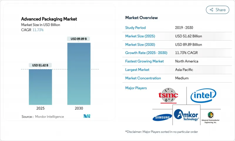
The advanced packaging market size was valued at USD 51.62 billion in 2025 and is forecast to expand at an 11.73% CAGR to reach USD 89.89 billion by 2030.
Demand outpaced earlier projections because heterogeneous integration became indispensable for artificial-intelligence (AI) processors that exceed the thermal and interconnect limits of conventional packages. In response, integrated-device manufacturers (IDMs) and outsourced semiconductor assembly and test (OSAT) providers accelerated capital spending, while governments earmarked large incentives to localize assembly capacity. The advanced packaging market also benefited from glass-core substrate R&D, panel-level processing pilots, and the rapid adoption of co-packaged optics in hyperscale data centers. Supply remained tight, however, as BT-resin substrate shortages and scarce engineering talent hindered timely capacity additions. Competitive intensity rose as foundries internalized packaging to secure end-to-end control of AI supply chains, squeezing traditional OSAT margins and prompting strategic specialization.
Global Advanced Packaging Market Trends and Insights
Rising demand for heterogeneous integration for AI and HPC
AI workloads require compute density and memory bandwidth unattainable with legacy packaging. TSMC's CoWoS platform integrates chiplets and high-bandwidth memory in a single structure, gaining rapid adoption among leading AI accelerator vendors. Samsung's SAINT technology achieved similar objectives using hybrid bonding that supports forthcoming HBM4 stacks, underscoring the strategic value of in-house advanced packaging. Thermal interface materials, specialized substrates, and active interposers raised package cost to 15-20% of the total semiconductor build-to-materials, up from 5-8% for mainstream CPUs. As a result, advanced packaging capacity became as critical as leading-edge fabs in determining time-to-market for AI systems. The advanced packaging market, therefore, grew in tandem with, rather than lagging, front-end process migrations.
Miniaturization of consumer devices boosting WLP adoption
Smartphones, wearables, and hearables consistently demand thinner profiles and higher functional density. Fan-out wafer-level packaging (FOWLP) enables multiple dies to be embedded in ultra-thin packages below 0.5 mm, supporting flagship mobile processors without compromising thermal performance. The shift from fan-in WLP to FOWLP reduced overall system cost by up to 25% because under-fill, wire-bonding, and laminate substrates were eliminated. Miniaturization also moved into implantable medical electronics, where dimensions are life-critical; leadless pacemakers benefited from WLP to cut device size by 93% while meeting stringent reliability targets. Consequently, consumer and medical demand created a recurring baseline that insulated the advanced packaging market from cyclical swings in PC end-markets.
High capital intensity constraining market entry
Tooling for 2.5D and 3D processes can cost USD 10-15 million per chamber, vastly exceeding the USD 3 million typical for legacy lines. TSMC budgeted USD 42 billion in 2025 capital outlays, of which a material share targeted advanced packaging expansions. Smaller OSATs, therefore, struggled to amortize investments across rapidly shrinking product life cycles, prompting niche specialization or defensive mergers. The elevated hurdle rate widened the technological gap between tier-one providers and regional followers, dampening fresh capacity in the advanced packaging market during 2024-2026.
Other drivers and restraints analyzed in the detailed report include:
- Government semiconductor subsidies accelerating infrastructure development
- EV power-electronics reliability transforming packaging requirements
- BT-resin substrate bottlenecks limiting production capacity
For complete list of drivers and restraints, kindly check the Table Of Contents.
Segment Analysis
Flip-chip packages retained leadership with 49.0% revenue in 2024, anchored by high-volume consumer and industrial applications. Yet 2.5D/3D configurations delivered the fastest gains, achieving a 13.2% CAGR outlook as AI accelerators demanded logic-to-memory proximity beyond flip-chip limits. The advanced packaging market size for 2.5D/3D solutions is forecast to reach USD 34.1 billion by 2030, equal to 38% of total platform revenue.
Samsung's SAINT platform attained sub-10 µm hybrid bonds, reducing signal latency by 30% and extending thermal headroom by 40% relative to wire-bonded stacks. TSMC's CoWoS ramped three additional lines in 2025 to clear a 12-month backlog. Embedded-die and fan-out WLP progressed as complementary options: embedded packages suited space-constrained automotive domains, while fan-out WLP captured 5G base-station and mmWave radar designs. Collectively, these dynamics embedded 2.5D/3D packaging at the center of next-generation device roadmaps, guaranteeing its role as the prime value driver inside the advanced packaging market.
Consumer electronics absorbed 40.0% of 2024 shipments, but its growth plateaued at single digits. In contrast, automotive and EV demand is projected to expand at a 12.4% CAGR, lifting its share of the advanced packaging market to 18% by 2030. The advanced packaging market size for automotive electronics is estimated to surpass USD 16 billion by the end of the forecast period.
EV traction inverters, on-board chargers, and domain controllers now specify automotive-grade fan-out, double-side cooled power modules, and over-molded system-in-package (SiP) assemblies. Data-center infrastructure provided another high-growth niche: AI servers utilize advanced packages with power densities reaching 1,000 W/cm2, dictating innovative thermal lid and under-fill chemistries. Healthcare, meanwhile, requires biocompatible coatings and hermetic enclosures, attributes that carry premium average selling prices and stable replacement demand. Cumulatively, these segment trends diversified revenue streams and reduced dependence on cyclical smartphone refresh cycles within the advanced packaging market.
Advanced Packaging Market is Segmented by Packaging Platform (Flip-Chip, Embedded Die, Fan-In WLP, and More), End-User Industry (Consumer Electronics, Automotive and EV, Data Center and HPC, and More), Device Architecture (2D IC, 2. 5D Interposer, and 3D IC), Interconnect Technology (Solder Bump, Copper Pillar, and Hybrid Bond), and Geography (North America, South America, Europe, Asia-Pacific, and Middle East and Africa).
Geography Analysis
Asia-Pacific generated 75.0% of 2024 revenue because Taiwan, South Korea, and mainland China house the bulk of front-end fabs and substrate suppliers. TSMC announced a USD 165 billion U.S. investment, reflecting a diversification strategy rather than the displacement of its Taiwan base, ensuring Asia retains leadership in the medium term. China's domestic OSATs delivered double-digit sales gains and expanded into automotive packaging, but tight controls on extreme-ultraviolet (EUV) tools limited their move into leading-edge wafer-fab processes.
North America emerged as the fastest-growing region at a 12.5% CAGR thanks to the CHIPS Act incentives. Amkor's USD 2 billion Arizona site will combine bump, wafer-level, and panel-level lines once fully ramped in 2027, providing the first large-scale outsourced option near U.S. system integrators. Intel, Apple, and NVIDIA pre-booked a portion of this capacity to de-risk geopolitical supply interruptions, redirecting meaningful volumes that historically flowed to East Asian OSATs. Consequently, the advanced packaging market now includes a credible North American supply node capable of high-volume AI product support.
Europe pursued specialization rather than volume leadership. onsemi's Czech facility addressed silicon-carbide devices for automotive power, aligning with local OEM electrification targets. Germany's Fraunhofer institutes led panel-level research, but manufacturers stayed cautious on green-field megasite commitments. Meanwhile, Singapore strengthened its hub role; Micron's HBM plant and KLA's process-control expansion created a vertically coherent ecosystem that supports AI memory and metrology under one jurisdiction. India introduced a 50% capital cost-sharing scheme, attracting proposals for advanced packaging pilots that promise medium-term upside yet remain contingent on talent availability.
Collectively, these developments diversified geographic risk for system OEMs and rebalanced the advanced packaging market. Even so, Asia-Pacific is forecast to maintain more than 60% share in 2030 because existing infrastructure, supply clusters, and economies of scale still surpass new regional entrants.
- Amkor Technology, Inc.
- Taiwan Semiconductor Manufacturing Company Limited
- Advanced Semiconductor Engineering, Inc.
- JCET Group Co., Ltd.
- Samsung Electronics Co., Ltd.
- Intel Corporation
- Chipbond Technology Corporation
- ChipMOS Technologies Inc.
- Powertech Technology Inc.
- TongFu Microelectronics Co., Ltd.
- Nepes Corporation
- STATS ChipPAC Pte. Ltd.
- Siliconware Precision Industries Co., Ltd.
- UTAC Holdings Ltd.
- Walton Advanced Engineering, Inc.
- Xintec Inc.
- Tianshui Huatian Technology Co., Ltd.
- King Yuan Electronics Co., Ltd.
- Signetics Corporation
- GlobalFoundries Inc.
- Semiconductor Manufacturing International Corporation
- SFA Semicon Co., Ltd.
- Nantong Fujitsu Microelectronics Co., Ltd.
- Hana Micron Inc.
- Unisem (M) Berhad
Additional Benefits:
- The market estimate (ME) sheet in Excel format
- 3 months of analyst support
TABLE OF CONTENTS
1 INTRODUCTION
- 1.1 Study Assumptions and Market Definition
- 1.2 Scope of the Study
2 RESEARCH METHODOLOGY
3 EXECUTIVE SUMMARY
4 MARKET LANDSCAPE
- 4.1 Market Overview
- 4.2 Impact of Macroeconomic Factors
- 4.3 Market Drivers
- 4.3.1 Rising demand for heterogeneous integration for AI and HPC
- 4.3.2 Miniaturization of consumer devices boosting WLP adoption
- 4.3.3 Government semiconductor subsidies (e.g., CHIPS, EU Chips Act)
- 4.3.4 EV power-electronics reliability needs (advanced power packages)
- 4.3.5 Emerging glass-core substrates enabling panel-level packaging
- 4.3.6 Co-packaged optics demand in hyperscale datacenters
- 4.4 Market Restraints
- 4.4.1 High capital intensity of advanced packaging lines
- 4.4.2 Industry consolidation squeezing outsourced margins
- 4.4.3 BT-resin substrate capacity bottlenecks
- 4.4.4 Shortage of advanced assembly talent
- 4.5 Value Chain Analysis
- 4.6 Regulatory Landscape
- 4.7 Technological Outlook
- 4.8 Porter's Five Forces Analysis
- 4.8.1 Threat of New Entrants
- 4.8.2 Bargaining Power of Buyers
- 4.8.3 Bargaining Power of Suppliers
- 4.8.4 Threat of Substitutes
- 4.8.5 Intensity of Rivalry
- 4.9 Investment Analysis
5 MARKET SIZE AND GROWTH FORECASTS (VALUE)
- 5.1 By Packaging Platform
- 5.1.1 Flip-Chip
- 5.1.2 Embedded Die
- 5.1.3 Fan-in WLP
- 5.1.4 Fan-out WLP
- 5.1.5 2.5D / 3D
- 5.2 By End-User Industry
- 5.2.1 Consumer Electronics
- 5.2.2 Automotive and EV
- 5.2.3 Data Center and HPC
- 5.2.4 Industrial and IoT
- 5.2.5 Healthcare / Med-tech
- 5.3 By Device Architecture
- 5.3.1 2D IC
- 5.3.2 2.5D Interposer
- 5.3.3 3D IC (TSV / Hybrid-Bond)
- 5.4 By Interconnect Technology
- 5.4.1 Solder Bump
- 5.4.2 Copper Pillar
- 5.4.3 Hybrid Bond
- 5.5 By Geography
- 5.5.1 North America
- 5.5.1.1 United States
- 5.5.1.2 Canada
- 5.5.1.3 Mexico
- 5.5.2 South America
- 5.5.2.1 Brazil
- 5.5.2.2 Argentina
- 5.5.2.3 Rest of South America
- 5.5.3 Europe
- 5.5.3.1 Germany
- 5.5.3.2 France
- 5.5.3.3 United Kingdom
- 5.5.3.4 Italy
- 5.5.3.5 Netherlands
- 5.5.3.6 Russia
- 5.5.3.7 Rest of Europe
- 5.5.4 Asia-Pacific
- 5.5.4.1 China
- 5.5.4.2 Taiwan
- 5.5.4.3 South Korea
- 5.5.4.4 Japan
- 5.5.4.5 Singapore
- 5.5.4.6 Malaysia
- 5.5.4.7 India
- 5.5.4.8 Rest of Asia-Pacific
- 5.5.5 Middle East and Africa
- 5.5.5.1 Middle East
- 5.5.5.1.1 Israel
- 5.5.5.1.2 United Arab Emirates
- 5.5.5.1.3 Saudi Arabia
- 5.5.5.1.4 Turkey
- 5.5.5.1.5 Rest of Middle East
- 5.5.5.2 Africa
- 5.5.5.2.1 South Africa
- 5.5.5.2.2 Nigeria
- 5.5.5.2.3 Rest of Africa
- 5.5.1 North America
6 COMPETITIVE LANDSCAPE
- 6.1 Market Concentration
- 6.2 Strategic Moves
- 6.3 Market Share Analysis
- 6.4 Company Profiles (includes Global level Overview, Market level overview, Core Segments, Financials as available, Strategic Information, Market Rank/Share for key companies, Products and Services, and Recent Developments)
- 6.4.1 Amkor Technology, Inc.
- 6.4.2 Taiwan Semiconductor Manufacturing Company Limited
- 6.4.3 Advanced Semiconductor Engineering, Inc.
- 6.4.4 JCET Group Co., Ltd.
- 6.4.5 Samsung Electronics Co., Ltd.
- 6.4.6 Intel Corporation
- 6.4.7 Chipbond Technology Corporation
- 6.4.8 ChipMOS Technologies Inc.
- 6.4.9 Powertech Technology Inc.
- 6.4.10 TongFu Microelectronics Co., Ltd.
- 6.4.11 Nepes Corporation
- 6.4.12 STATS ChipPAC Pte. Ltd.
- 6.4.13 Siliconware Precision Industries Co., Ltd.
- 6.4.14 UTAC Holdings Ltd.
- 6.4.15 Walton Advanced Engineering, Inc.
- 6.4.16 Xintec Inc.
- 6.4.17 Tianshui Huatian Technology Co., Ltd.
- 6.4.18 King Yuan Electronics Co., Ltd.
- 6.4.19 Signetics Corporation
- 6.4.20 GlobalFoundries Inc.
- 6.4.21 Semiconductor Manufacturing International Corporation
- 6.4.22 SFA Semicon Co., Ltd.
- 6.4.23 Nantong Fujitsu Microelectronics Co., Ltd.
- 6.4.24 Hana Micron Inc.
- 6.4.25 Unisem (M) Berhad
7 MARKET OPPORTUNITIES AND FUTURE OUTLOOK
- 7.1 White-space and Unmet-Need Assessment

