
PUBLISHER: Mordor Intelligence | PRODUCT CODE: 1851389

PUBLISHER: Mordor Intelligence | PRODUCT CODE: 1851389
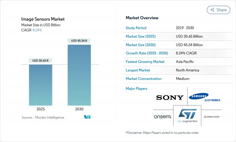
Image Sensors - Market Share Analysis, Industry Trends & Statistics, Growth Forecasts (2025 - 2030)
The image sensor market reached USD 30.65 billion in 2025 and is projected to expand to USD 45.54 billion by 2030, translating to an 8.24% CAGR over the forecast period.
Growth reflects a confluence of automotive safety mandates, sophisticated multi-camera smartphones, and industrial automation needs that are reshaping semiconductor demand. Vehicle makers are equipping an average of 8 cameras per car in 2025 and plan to add 12 cameras by 2028, accelerating sensor volumes and ASP expansion. CMOS devices capture 93% of 2024 unit shipments because of low-power on-chip processing, while stacked back-side-illuminated (BSI) designs, scaling at a 55% CAGR to 2030, unlock higher dynamic range and AI computation at the edge. The 4-12 MP resolution bracket dominates with 32% revenue because it balances image quality and cost for mainstream consumer and industrial use. Competitive intensity is rising as Sony, Samsung, OmniVision and onsemi defend share against new entrants amid geopolitical export controls, 300 mm wafer scarcity, and thermal-noise barriers that slow sub-micron pixel shrink.
Global Image Sensors Market Trends and Insights
Automotive-grade Image Sensors Fueling ADAS & Autonomous Deployment
Automotive safety regulation is shifting cameras from premium options to mandated equipment, transforming the image sensor market. onsemi's Hyperlux AR0823AT won Subaru's next-gen EyeSight stereo-camera slot, meeting ASIL-C targets for autonomous decision making. Canon's prototype 410 MP sensor processes 3,280 MP/s, showing that modern sensors are computational platforms, not passive imagers. Sony projects a 6.68-fold jump in car camera nodes between 2019 and 2030, highlighting sustained OEM pull for high-dynamic-range, low-latency parts. HDR, LED-flicker mitigation and functional-safety IP now come standard, positioning automotive imagers as critical safety infrastructure.
Penetration of Multi-Camera Smartphones with High-Resolution CMOS BSI Sensors in Asia
Asia's handset ecosystem keeps driving pixel-architecture breakthroughs. Samsung converted its Hwaseong line to stacked CIS fabrication starting 2025, chasing premium iPhone design wins. Its 3-layer sensor splits photodiode, transfer and logic strata, boosting dynamic range while shrinking footprint. OmniVision's OV50X delivers 110 dB single-exposure HDR with 1.6 µm pixels, proving Asian suppliers now lead in low-light computational imaging. The shift from megapixel race to image quality underscores a mature smartphone cycle where advanced BSI and AI ISP integration differentiate user experience.
Supply-Chain Concentration in 300 mm Wafer Fabs Creating Price Volatility
SEMI records 30 million wafers-per-month capacity in 2024, yet production clusters around a handful of Asian foundries, amplifying shortages during demand spikes. Image sensor lines now compete with high-margin AI accelerators for the same 300 mm tools, lifting die prices and lengthening lead times. McKinsey observes that 60% of specialty chemicals needed for lithography lack local US supply, adding upstream risk. Until Arizona and European fabs reach volume after 2026, price swings will compress margins across the image sensor market.
Other drivers and restraints analyzed in the detailed report include:
- Growing Adoption of SWIR/NIR Sensors in Precision Agriculture & Industrial Inspection
- Edge-AI-Enabled Vision Modules Accelerating IoT & Smart City Projects
- Thermal Noise & Power Limits in Sub-Micron Pixel Shrink Challenging Further Resolution Gains
For complete list of drivers and restraints, kindly check the Table Of Contents.
Segment Analysis
CMOS sensors owned 93% of unit shipments in 2024, underscoring their low-power logic integration and per-wafer economics. The image sensor market size for CMOS reached USD 28.7 billion in 2025, dwarfing CCD revenues. Column-parallel ADC and backside wiring lift frame rate while shrinking die area, letting vendors ship 5-7 billion parts yearly for phones alone. Scientific and medical instruments continue ordering CCDs for ultra-low dark current, yet fab investments trend to CMOS, ensuring its share rises. Samsung's 3-layer stack demonstrates how separating photodiode, transfer and logic planes lifts quantum efficiency and reduces crosstalk, cementing CMOS leadership.
Second-generation stacked CIS improves redundancy and defect management, driving a projected 10.2% unit CAGR for CMOS through 2030. This momentum allows new entrants from China and India to license mature-node 65 nm flows and still launch competitive imagers for automotive surround-view. The image sensor market remains anchored on CMOS innovation as foundries add buried oxide isolation and hybrid bonding lines dedicated to photonics modules.
Stacked BSI shipments are growing at 55% CAGR because vertical integration circumvents 2-D scaling limits. Separating photodiode and logic layers permits larger light-collection areas without enlarging die, yielding 1.5-2 EV sensitivity uplift. Canon's 410 MP stacked full-frame sensor reads 3,280 MP/s via 40 parallel lanes, showing high-performance potential. Manufacturing yields have risen as wafer-to-wafer hybrid bonding moves from pilot to 24/7 production, cutting cost by 30% versus through-silicon-via stacking.
Within the image sensor market, stacked BSI is forecast to command USD 25.9 billion of image sensor market size by 2030, underpinned by smartphone and automotive ADAS volume ramps. Front-side and conventional BSI remain viable in low-tier devices where cost dominates, but premium makers now align roadmaps around multi-layer stacks that embed ISP blocks, SDRAM and AI accelerators under the pixel matrix, driving system-in-package convergence.
The Image Sensor Market Report is Segmented by Type (CMOS, CCD), Processing Technology (Front-Side Illuminated, Back-Side Illuminated, and More), Shutter Type (Rolling, Global), Spectrum (Visible, Near-Infrared, and More), Resolution (Less Than1 MP, 1-3 MP, and More), End-User Industry (Consumer Electronics, Automotive, Industrial, and More), and Geography. The Market Forecasts are Provided in Terms of Value (USD).
Geography Analysis
North America remains the largest regional buyer measured in revenue because ADAS regulations and defense procurements drive high-spec ASP. The United States finalized automatic emergency braking rules that implicitly require forward-facing cameras in all light vehicles from 2029, locking long-tail demand. Canada's Tier-1 suppliers cluster around Ontario's automotive corridor, and Mexico hosts module assembly for US OEMs. The region's push for semiconductor sovereignty spurred TSMC's USD 165 billion Arizona megafab, anticipated to supply mature-node CIS wafers post-2027.
Europe emphasizes privacy-first smart cities, funding edge-AI image sensors via the Chips Act. ams OSRAM's EUR 588 million Austrian expansion will feed both automotive lidar and municipal traffic nodes. Germany and France enforce Euro-NCAP camera benchmarks that trickle to suppliers across the continent. Local regulations cap cloud storage of facial data, encouraging in-sensor encryption and on-device inference, cultivating a premium for secure image sensor market designs.
Asia-Pacific houses most wafer capacity and posts the fastest shipment growth. Japan's Sony aims for 43% automotive CMOS share by 2026 on the back of Tier-1 alliances. South Korea's Samsung is retooling Hwaseong for additional 200,000 wafers-per-month CIS output to backfill smartphone and AR/VR cameras. China increases remote-sensing demand for its Jilin-1 constellation yet faces US export controls on advanced 28 nm CIS nodes, prompting domestic foundries to accelerate mature-process investments. India emerges as a consumption-driven market for automotive dash-cams and low-cost phones, while Israel develops niche defense imagers in GaAs fabs, extending regional diversity.
- Sony Group Corp.
- Samsung Electronics Co., Ltd.
- OmniVision Technologies, Inc.
- STMicroelectronics N.V.
- ON Semiconductor Corporation
- Canon Inc.
- Panasonic Holdings Corporation
- Teledyne DALSA Inc.
- ams OSRAM AG
- SK hynix Inc.
- GalaxyCore Inc.
- Hamamatsu Photonics K.K.
- SmartSens Technology
- PixArt Imaging Inc.
- Himax Technologies, Inc.
- Tower Semiconductor Ltd.
- Teledyne e2v
- Gpixel Inc.
- Forza Silicon Corp.
- Toshiba Electronic Devices and Storage Corp.
- Pyxalis S.A.
Additional Benefits:
- The market estimate (ME) sheet in Excel format
- 3 months of analyst support
TABLE OF CONTENTS
1 INTRODUCTION
- 1.1 Study Assumptions and Market Definition
- 1.2 Scope of the Study
2 RESEARCH METHODOLOGY
3 EXECUTIVE SUMMARY
4 MARKET LANDSCAPE
- 4.1 Market Overview
- 4.2 Market Drivers
- 4.2.1 Automotive-grade Image Sensors Fueling ADAS and Autonomous Deployment
- 4.2.2 Penetration of Multi-Camera Smartphones with High-Resolution CMOS BSI Sensors in Asia
- 4.2.3 Growing Adoption of SWIR/NIR Sensors in Precision Agriculture and Industrial Inspection
- 4.2.4 Edge-AI-Enabled Vision Modules Accelerating IoT and Smart City Projects, Especially in Europe
- 4.2.5 Rising Demand for Global Shutter Sensors in AR/VR Wearables
- 4.2.6 Government Safety Mandates for ADAS Cameras in North America and Japan
- 4.3 Market Restraints
- 4.3.1 Supply-Chain Concentration in 300 mm Wafer Fabs Creating Price Volatility
- 4.3.2 Thermal Noise and Power Limits in Sub-Micron Pixel Shrink Challenging Further Resolution Gains
- 4.3.3 Export Controls on Advanced Imaging Chips Affecting China-Based OEMs
- 4.3.4 High Integration Cost of SWIR Sensors Limiting Consumer Electronics Adoption
- 4.4 Value / Supply-Chain Analysis
- 4.5 Regulatory Outlook
- 4.6 Technological Outlook
- 4.7 Porter's Five Forces Analysis
- 4.7.1 Bargaining Power of Suppliers
- 4.7.2 Bargaining Power of Consumers
- 4.7.3 Threat of New Entrants
- 4.7.4 Threat of Substitutes
- 4.7.5 Intensity of Competitive Rivalry
- 4.8 Assessment on the Impact of COVID-19 and Israel-Gaza Conflict
5 MARKET SIZE AND GROWTH FORECASTS (VALUE)
- 5.1 By Type
- 5.1.1 CMOS
- 5.1.2 CCD
- 5.2 By Processing Technology
- 5.2.1 Front-Side Illuminated (FSI)
- 5.2.2 Back-Side Illuminated (BSI)
- 5.2.3 Stacked BSI
- 5.3 By Shutter Type
- 5.3.1 Rolling Shutter
- 5.3.2 Global Shutter
- 5.4 By Spectrum
- 5.4.1 Visible (RGB)
- 5.4.2 Near-Infrared (NIR)
- 5.4.3 Short-Wave Infrared (SWIR)
- 5.4.4 X-ray / UV
- 5.5 By Resolution
- 5.5.1 Less than 1 MP
- 5.5.2 1-3 MP
- 5.5.3 4-12 MP
- 5.5.4 13-24 MP
- 5.5.5 Greater than or Equal to 25 MP
- 5.6 By End-User Industry
- 5.6.1 Consumer Electronics
- 5.6.2 Automotive and Transportation
- 5.6.3 Industrial Automation and Robotics
- 5.6.4 Security and Surveillance
- 5.6.5 Healthcare and Life Sciences
- 5.6.6 Aerospace and Defense
- 5.6.7 Others (Smart City, Agriculture, Marine)
- 5.7 By Geography
- 5.7.1 North America
- 5.7.1.1 United States
- 5.7.1.2 Canada
- 5.7.1.3 Mexico
- 5.7.2 Europe
- 5.7.2.1 United Kingdom
- 5.7.2.2 Germany
- 5.7.2.3 France
- 5.7.2.4 Italy
- 5.7.2.5 Rest of Europe
- 5.7.3 Asia-Pacific
- 5.7.3.1 China
- 5.7.3.2 Japan
- 5.7.3.3 India
- 5.7.3.4 South Korea
- 5.7.3.5 Rest of Asia-Pacific
- 5.7.4 Middle East
- 5.7.4.1 Israel
- 5.7.4.2 Saudi Arabia
- 5.7.4.3 United Arab Emirates
- 5.7.4.4 Turkey
- 5.7.4.5 Rest of Middle East
- 5.7.5 Africa
- 5.7.5.1 South Africa
- 5.7.5.2 Egypt
- 5.7.5.3 Rest of Africa
- 5.7.6 South America
- 5.7.6.1 Brazil
- 5.7.6.2 Argentina
- 5.7.6.3 Rest of South America
- 5.7.1 North America
6 COMPETITIVE LANDSCAPE
- 6.1 Market Concentration
- 6.2 Strategic Moves
- 6.3 Market Share Analysis
- 6.4 Company Profiles (includes Global level Overview, Market level overview, Core Segments, Financials as available, Strategic Information, Market Rank/Share, Products and Services, Recent Developments)
- 6.4.1 Sony Group Corp.
- 6.4.2 Samsung Electronics Co., Ltd.
- 6.4.3 OmniVision Technologies, Inc.
- 6.4.4 STMicroelectronics N.V.
- 6.4.5 ON Semiconductor Corporation
- 6.4.6 Canon Inc.
- 6.4.7 Panasonic Holdings Corporation
- 6.4.8 Teledyne DALSA Inc.
- 6.4.9 ams OSRAM AG
- 6.4.10 SK hynix Inc.
- 6.4.11 GalaxyCore Inc.
- 6.4.12 Hamamatsu Photonics K.K.
- 6.4.13 SmartSens Technology
- 6.4.14 PixArt Imaging Inc.
- 6.4.15 Himax Technologies, Inc.
- 6.4.16 Tower Semiconductor Ltd.
- 6.4.17 Teledyne e2v
- 6.4.18 Gpixel Inc.
- 6.4.19 Forza Silicon Corp.
- 6.4.20 Toshiba Electronic Devices and Storage Corp.
- 6.4.21 Pyxalis S.A.
7 MARKET OPPORTUNITIES AND FUTURE OUTLOOK
- 7.1 White-space and Unmet-Need Assessment

