
PUBLISHER: Mordor Intelligence | PRODUCT CODE: 1851742

PUBLISHER: Mordor Intelligence | PRODUCT CODE: 1851742
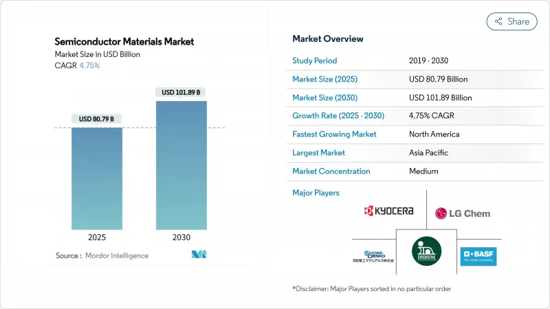
Semiconductor Materials - Market Share Analysis, Industry Trends & Statistics, Growth Forecasts (2025 - 2030)
The semiconductor materials market size reached USD 80.79 billion in 2025 and is projected to expand to USD 101.89 billion by 2030, advancing at a 4.75% CAGR during the forecast period.
Continued AI-optimized architectures and automotive electrification are reshaping material requirements as traditional silicon approaches fundamental physics limits. Advanced packaging materials are accelerating at an 11.8% CAGR because chiplet designs and 3D stacking architectures need novel interconnect and thermal solutions. Fabrication materials still dominate with a 63% revenue share in 2024, but value creation is migrating downstream where packaging innovation increasingly shapes system performance. Demand is also buoyed by the pivot to wide-bandgap power devices in electric vehicles and by strategic reshoring programs that incentivize domestic material supply chains in North America and Europe. Geopolitical tensions surrounding critical chemicals-most visibly Japan's 2019 hydrogen-fluoride curbs-have underscored the importance of diversified sourcing strategies.
Global Semiconductor Materials Market Trends and Insights
Digitalization-led Fab Expansions
The USD 400 billion earmarked for 300 mm fab equipment through 2027 represents the largest capacity build-out in semiconductor history. Texas Instruments alone has committed USD 60 billion across seven US fabs, while Micron plans USD 200 billion in domestic memory facilities. . Each advanced fab consumes 40% more specialty chemicals per wafer than the previous generation, intensifying pressure on suppliers to scale ultra-high-purity production in multiple geographies.
5G/AI End-Device Proliferation
AI accelerators push unprecedented bandwidth and thermal envelopes, tripling materials spend per packaged chip relative to conventional processors. HBM stacks rely on through-silicon-via copper pillars and ultra-thin die-attach films that demand silver-rich formulations. Fujifilm has targeted JPY 500 billion in semiconductor-materials revenue by 2030, largely from EUV photoresists tailored for AI-centric nodes. On the automotive side, LG Chem's high-performance silver paste for SiC power modules exemplifies how AI-driven mobility raises both temperature and voltage requirements.
Cyclicality of Consumer Electronics
The semiconductor packaging materials segment fell 15.5% in 2023 before rebounding in 2024, illustrating how smartphone and PC slowdowns ripple quickly through chemical demand. Inventory swings of up to 30% within a quarter pressure suppliers devoted to high-volume consumer lines. Diversification into automotive, industrial and infrastructure is mitigating but not eliminating this volatility. The advent of AI-enhanced consumer devices may lower cyclical amplitude yet introduce fresh forecasting complexity as bill-of-materials inflation replaces unit growth as the primary revenue lever.
Other drivers and restraints analyzed in the detailed report include:
- Automotive Electrification & ADAS
- Advanced-Node Investments (<=5 nm)
- High Capital Intensity for New Chemistries
For complete list of drivers and restraints, kindly check the Table Of Contents.
Segment Analysis
Fabrication materials commanded 63% revenue in 2024, reflecting the hundreds of etch, deposition and planarization steps per wafer. Wet chemicals, electronic gases and CMP consumables form the largest cost pools. In value terms, this slice of the semiconductor materials market size equated to more than USD 50 billion in 2024. Advanced packaging, while smaller today, is scaling at a 9.2% CAGR as chiplet partitioning pushes metallization density and thermal-interface performance beyond organic laminate capabilities. The semiconductor materials market is therefore tilting toward substrates, under-fills and mold compounds engineered for multi-die architectures, supported by an 11.8% CAGR in packaging raw materials.
The pivot also recasts industry power dynamics. Fabrication suppliers benefit from scale but face flatter growth curves, whereas packaging innovators can secure design-in wins with higher long-term elasticity. For instance, BT-resin-based substrates enable finer lines and spaces than traditional FR-4, unlocking performance gains in AI accelerators. Materials vendors that straddle both process nodes and package architectures gain cross-cycle resilience, capturing spend both at wafer start and at module finish.
Wet-process chemicals remained the largest material class, representing 24% of 2024 spend, thanks to their universal role in cleaning, stripping and etching. Ongoing node migration increases dosage intensity-leading-edge fabs use 40% more acids and bases per wafer than 28 nm lines. Specialty gases, including hydrogen fluoride and nitrogen trifluoride, follow closely in value and face geopolitical supply scrutiny. Japan's 2019 export restrictions slashed hydrogen-fluoride shipments to South Korea by 96.8%, prompting rapid dual-sourcing across Taiwan, Belgium and the United States.
CMP slurries and pads show steady upticks as the number of planarization steps rises with each design shrink. Photoresists evolve with EUV adoption; new polymer platforms must endure 13.5 nm photon bombardment without line-edge roughness degradation. Substrate innovation is broadening beyond 300 mm silicon to include high-quality SiC boules and 200 mm GaN wafers for power devices. Collectively, these shifts are reshaping the semiconductor materials market, forcing suppliers to balance purity, sustainability and cost.
Semiconductor Materials Market Segmented by Application (Fabrication, Packaging), Material Type (Wafer Substrates, Specialty and More), End-User Industry (Consumer Electronics, Telecommunications, and More), Technology Node, Fab Ownership (IDM, Pure-Play and More), and Geography. The Market Forecasts are Provided in Terms of Value (USD).
Geography Analysis
Asia-Pacific commanded 55% of 2024 revenue owing to its dense manufacturing ecosystem across Taiwan, South Korea, Japan and mainland China. However, the region's concentration exposes supply chains to export-control shocks as evidenced by the 2019 hydrogen-fluoride episode. Japanese suppliers are fortifying resilience with USD 545 million in new chemical plants and targeted acquisitions to secure local control of high-purity lines.
North America is the fastest-growing territory, advancing at a 6.4% CAGR through 2030 on the back of USD 52 billion in CHIPS Act incentives. Intel, TSMC and Samsung are collectively building more than 20 million wafers per-year of capacity, catalysing parallel investments from Air Liquide (USD 250 million in Idaho) and Entegris (USD 75 million for Colorado Springs). Domestic packaging and test expansions are shortening lead times and stimulating demand for solder-ball alloys and advanced substrates produced within the region. Environmental regulators are simultaneously accelerating adoption of PFAS-free chemistries, giving local innovators a foothold.
Europe is leveraging its Chips Act to reach 20% global share by 2030. Merck, BASF and Linde are upgrading ultra-purity sulfuric and ammonia lines to support new fabs in Germany and France. India is emerging as a secondary hub for mature-node and OSAT work, attracting specialty-gas makers with greenfield investments. The Middle East and Africa remain nascent but could benefit from sovereign efforts to localize power-device assembly tied to renewable energy projects. Collectively these moves are geographically redistributing the semiconductor materials market, increasing total spend through redundancy while easing geopolitical risk.
- DuPont de Nemours, Inc.
- BASF SE
- Showa Denko Materials Co., Ltd.
- Tokyo Ohka Kogyo Co., Ltd.
- Shin-Etsu Chemical Co., Ltd.
- Merck KGaA (EMD Electronics)
- LG Chem Ltd.
- Henkel AG and Co. KGaA
- Indium Corporation
- SUMCO Corporation
- JSR Corporation
- KYOCERA Corporation
- Versum Materials (Merck)
- Caplinq Europe B.V.
- Nichia Corporation
- International Quantum Epitaxy Plc.
- Sumitomo Chemical Co., Ltd.
- DOW Inc.
- Air Liquide Electronics
- Linde plc Electronics
- SK Materials Co., Ltd.
Additional Benefits:
- The market estimate (ME) sheet in Excel format
- 3 months of analyst support
TABLE OF CONTENTS
1 INTRODUCTION
- 1.1 Study Assumptions and Market Definition
- 1.2 Scope of the Study
2 RESEARCH METHODOLOGY
3 EXECUTIVE SUMMARY
4 MARKET LANDSCAPE
- 4.1 Market Overview
- 4.2 Market Drivers
- 4.2.1 Digitalisation-led fab expansions
- 4.2.2 5G/AI end-device proliferation
- 4.2.3 Automotive electrification and ADAS
- 4.2.4 Advanced-node investments (5 nm)
- 4.2.5 Chiplet and heterogenous integration BOM uplift
- 4.2.6 Regionalisation-driven safety-stock policies
- 4.3 Market Restraints
- 4.3.1 Cyclicality of consumer electronics
- 4.3.2 High capital intensity for new chemistries
- 4.3.3 Environmental regulations on PFAS chemistries
- 4.3.4 Hydrogen fluoride supply security in APAC
- 4.4 Value / Supply Chain Analysis
- 4.5 Regulatory Landscape
- 4.6 Technological Outlook
- 4.7 Porter's Five Forces
- 4.7.1 Bargaining Power of Suppliers
- 4.7.2 Bargaining Power of Consumers
- 4.7.3 Threat of New Entrants
- 4.7.4 Threat of Substitutes
- 4.7.5 Intensity of Competitive Rivalry
5 MARKET SIZE AND GROWTH FORECASTS (VALUE)
- 5.1 By Application
- 5.1.1 Fabrication
- 5.1.1.1 Process Chemicals
- 5.1.1.2 Photomasks
- 5.1.1.3 Electronic Gases
- 5.1.1.4 Photoresist Ancillaries
- 5.1.1.5 Sputtering Targets
- 5.1.1.6 Silicon
- 5.1.1.7 Other Fabrication Materials
- 5.1.2 Packaging
- 5.1.2.1 Substrates
- 5.1.2.2 Lead-frames
- 5.1.2.3 Ceramic Packages
- 5.1.2.4 Bonding Wire
- 5.1.2.5 Encapsulation Resins
- 5.1.2.6 Die-Attach Materials
- 5.1.2.7 Other Packaging Materials
- 5.1.1 Fabrication
- 5.2 By Material Type
- 5.2.1 Wafer Substrates
- 5.2.2 Specialty Gases
- 5.2.3 Wet Process Chemicals
- 5.2.4 Photoresists and Ancillaries
- 5.2.5 CMP Slurries and Pads
- 5.2.6 Advanced Packaging Materials
- 5.3 By End-User Industry
- 5.3.1 Consumer Electronics
- 5.3.2 Telecommunications
- 5.3.3 Manufacturing / Industrial IoT
- 5.3.4 Automotive
- 5.3.5 Energy and Utility
- 5.3.6 Others
- 5.4 By Technology Node
- 5.4.1 More than 45 nm
- 5.4.2 28-45 nm
- 5.4.3 14-22 nm
- 5.4.4 7-10 nm
- 5.4.5 Less than 5 nm
- 5.5 By Fab Ownership
- 5.5.1 IDM
- 5.5.2 Pure-play Foundry
- 5.5.3 Fabless (materials purchased via foundry)
- 5.5.4 OSAT / Assembly and Test
- 5.6 By Geography
- 5.6.1 North America
- 5.6.1.1 United States
- 5.6.1.2 Canada
- 5.6.1.3 Mexico
- 5.6.2 Europe
- 5.6.2.1 United Kingdom
- 5.6.2.2 Germany
- 5.6.2.3 France
- 5.6.2.4 Italy
- 5.6.2.5 Rest of Europe
- 5.6.3 Asia-Pacific
- 5.6.3.1 China
- 5.6.3.2 Japan
- 5.6.3.3 India
- 5.6.3.4 South Korea
- 5.6.3.5 Rest of Asia-Pacific
- 5.6.4 Middle East
- 5.6.4.1 Israel
- 5.6.4.2 Saudi Arabia
- 5.6.4.3 United Arab Emirates
- 5.6.4.4 Turkey
- 5.6.4.5 Rest of Middle East
- 5.6.5 Africa
- 5.6.5.1 South Africa
- 5.6.5.2 Egypt
- 5.6.5.3 Rest of Africa
- 5.6.6 South America
- 5.6.6.1 Brazil
- 5.6.6.2 Argentina
- 5.6.6.3 Rest of South America
- 5.6.1 North America
6 COMPETITIVE LANDSCAPE
- 6.1 Market Concentration
- 6.2 Strategic Moves
- 6.3 Market Share Analysis
- 6.4 Company Profiles (includes Global level Overview, Market level overview, Core Segments, Financials as available, Strategic Information, Market Rank/Share for key companies, Products and Services, and Recent Developments)
- 6.4.1 DuPont de Nemours, Inc.
- 6.4.2 BASF SE
- 6.4.3 Showa Denko Materials Co., Ltd.
- 6.4.4 Tokyo Ohka Kogyo Co., Ltd.
- 6.4.5 Shin-Etsu Chemical Co., Ltd.
- 6.4.6 Merck KGaA (EMD Electronics)
- 6.4.7 LG Chem Ltd.
- 6.4.8 Henkel AG and Co. KGaA
- 6.4.9 Indium Corporation
- 6.4.10 SUMCO Corporation
- 6.4.11 JSR Corporation
- 6.4.12 KYOCERA Corporation
- 6.4.13 Versum Materials (Merck)
- 6.4.14 Caplinq Europe B.V.
- 6.4.15 Nichia Corporation
- 6.4.16 International Quantum Epitaxy Plc.
- 6.4.17 Sumitomo Chemical Co., Ltd.
- 6.4.18 DOW Inc.
- 6.4.19 Air Liquide Electronics
- 6.4.20 Linde plc Electronics
- 6.4.21 SK Materials Co., Ltd.
7 MARKET OPPORTUNITIES AND FUTURE OUTLOOK
- 7.1 White-space and Unmet-Need Assessment

