
PUBLISHER: Mordor Intelligence | PRODUCT CODE: 1910505

PUBLISHER: Mordor Intelligence | PRODUCT CODE: 1910505
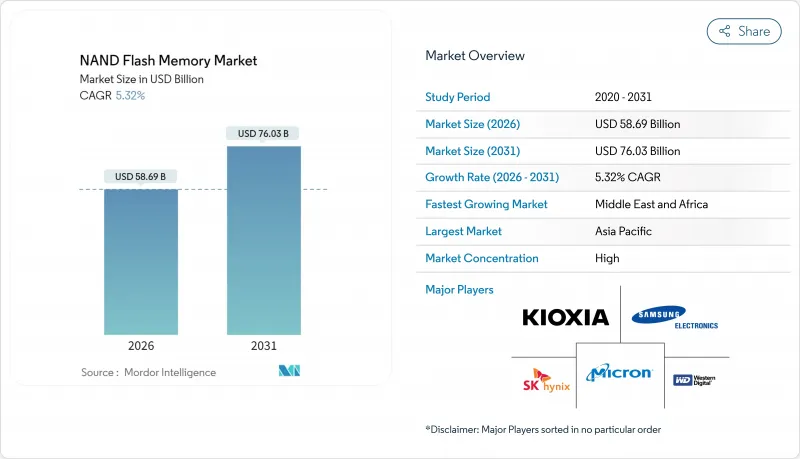
NAND Flash Memory - Market Share Analysis, Industry Trends & Statistics, Growth Forecasts (2026 - 2031)
NAND flash memory market size in 2026 is estimated at USD 58.69 billion, growing from 2025 value of USD 55.73 billion with 2031 projections showing USD 76.03 billion, growing at 5.32% CAGR over 2026-2031.
This steady expansion is powered by hyperscale data-center capital spending on artificial-intelligence training clusters, the transition of client PCs and game consoles to solid-state storage, and vertically-scaled 3D architectures that keep cost-per-bit on a declining path. At the same time, national incentives to localize semiconductor fabrication, especially in the United States and Saudi Arabia, are strengthening regional supply resilience. Layer-count breakthroughs above 300 layers and PCIe 5.0 adoption are shortening replacement cycles for both enterprise and consumer SSDs. The confluence of 5G rollouts and massive IoT endpoints further widens addressable demand, positioning the NAND flash memory market for durable mid-single-digit growth horizons.
Global NAND Flash Memory Market Trends and Insights
Data-center AI/ML storage surge
Hyperscale operators are redesigning storage hierarchies so that NVMe SSD pools sit closer to GPU clusters, sustaining multi-gigabyte-per-second throughput for retrieval-augmented generation workloads. Western Digital estimates cumulative demand of 19,000 petabytes of NAND by 2029 for 5G-enabled endpoints alone, underscoring flash's role in bridging memory and cold-storage performance gaps. Procurement roadmaps increasingly favor 30 TB to 100 TB enterprise drives, a shift visible in Samsung's 128 TB BM1743 SSD showcased in 2024. The resulting pull-through effect accelerates layer-count innovation and controller-level compression techniques that sustain the NAND flash memory market momentum.
5G and massive-IoT device proliferation
Standalone 5G deployments unlock edge analytics use cases, smart factories, connected cars, and smart grids that mandate local non-volatile storage for real-time decision engines. Western Digital's white paper anticipates a NOR-to-NAND crossover within industrial modules as capacities climb above 8 GB. Semiconductor roadmaps now prioritize extended-temperature QLC die and automotive-qualified NVMe designs, broadening the NAND flash memory market footprint across transportation and infrastructure domains.
Endurance limits of high-density cells
QLC's 1,000-3,000 program/erase thresholds remain insufficient for log-heavy databases, forcing over-provisioning that erodes cost benefits. Hackaday notes the physics ceiling approaching as electron-trap wear accelerates in 300-layer stacks. Although advanced error-correction and wear-leveling algorithms offset degradation, alternate memories such as PLC or cross-point remain on the horizon, tempering portions of the NAND flash memory market until longevity is proven.
Other drivers and restraints analyzed in the detailed report include:
- PC/Console transition from HDD to SSD
- Enterprise pivot to cost-efficient QLC SSDs
- Pricing cyclicality and cap-ex burden
For complete list of drivers and restraints, kindly check the Table Of Contents.
Segment Analysis
The NAND flash memory market size for TLC devices held a 63.58% market share with the strength of balanced endurance and cost. QLC, however, is accelerating at 6.35% CAGR as hyperscalers validate its 8-16X density advantage for AI data-lakes, which lifts the overall NAND flash memory market share allocated to QLC by 2031. Samsung's 280-layer QLC prototype signals a roadmap to 16 TB single-sided M.2 drives, shrinking rack footprints while meeting throughput rules for inference clusters. Controller-level SLC-cache techniques and on-die ECC are narrowing the latency gap with TLC, encouraging broader workloads such as VOD libraries and backup repositories to migrate. TLC will retain primacy in write-intensive ERP and OLTP environments where its 10,000-plus cycle rating secures predictable quality-of-service.
In consumer notebooks, TLC's favorable power profile sustains its install base, but falling QLC cost-per-bit is already pressuring mid-range SKUs. Micron's sixth-gen QLC exhibits 34% lower read latency than first-gen samples, eroding the perceived performance divide. As firmware-defined endurance mitigation matures, OEMs will likely introduce tiered offerings where high-capacity SKUs employ QLC, while premium lines continue on advanced TLC nodes. This interplay keeps both technologies central to the NAND flash memory market over the forecast horizon.
The shift from planar to vertical stacking is virtually complete: 3D NAND commanded 86.85% of the NAND flash memory market share in 2025. Layer-count breakthroughs, SK Hynix's commercial 321-layer TLC and Samsung's 400-plus-layer V-NAND, signal confident scaling beyond the 500-layer watermark before decade-end. The economic logic is clear; vertical scaling adds capacity without shrinking cell size, sidestepping lithography constraints. 2D NAND survives in niche aerospace and defense modules where ultra-low-latency writes outweigh capacity.
Layer additions do stress interconnect resistance and cell-to-cell interference. To overcome this, Kioxia's CMOS-bonded-array strategy decouples peripheral circuits, boosting I/O efficiency and improving yield in ultra-tall stacks. Samsung's exploration of hafnia ferroelectrics for creamy-interface gates pursues a similar aim: maintain threshold-voltage margins even as stack height extends.
The NAND Flash Memory Report is Segmented by Type (SLC (Single-Level Cell), MLC (Multi-Level Cell), TLC (Triple-Level Cell), and QLC (Quad-Level Cell)), Structure (2D (Planar) NAND, and 3D NAND), Interface (SATA, Pcie / NVMe, and UFS / EMMC), Application (Smartphones, Solid-State Drives (PC and Console), Enterprise / Data-Center SSD, and More), and Geography. The Market Forecasts are Provided in Terms of Value (USD).
Geography Analysis
Asia-Pacific contributed 55.40% of sales in 2025, anchored by South Korea's vertically-integrated champions and China's colossal device assembly base. Samsung's mass production of 9th-generation V-NAND (286 layers) and SK Hynix's 321-layer TLC line affirm the region's technology lead. Beijing's domestic champion YMTC pushes 232-layer QLC nodes despite export-control constraints, illustrating indigenous capacity expansion that preserves Asia-Pacific's outsized influence on the NAND flash memory market.
North America sits second on revenue league tables, propelled by cloud capital-expenditure intensity. The CHIPS and Science Act bankrolls Micron's USD 125 billion state-side megafab roadmap, lifting U.S. advanced-memory self-sufficiency by 2035. Canada contributes controller-IP design talent, while Mexico scales module-level assembly lines under USMCA provisions, together reinforcing regional supply diversification.
Europe registers mid-single-digit share, constrained by limited memory wafer fabrication. Nonetheless, automotive and industrial OEMs in Germany and France generate robust demand for auto-grade NVMe modules. Sustainability directives such as the European Green Deal pivot buyers toward power-efficient PCIe 5.0 SSDs that lower rack energy density, a niche European fabs aim to capture through next-generation 3D NAND nodes with under-3 pJ/bit read energy footprints.
The Middle East and Africa present the highest growth rate at 8.21% CAGR. Saudi Arabia's Vision 2030 underwrites wafer-to-back-end complexes around Riyadh, while Abu Dhabi's sovereign investors explore joint-ventures with controller specialists to bootstrap a regional supply chain. Ample renewable-energy pipelines and attractive tax regimes draw packaging partners, setting the stage for localized production that boosts the NAND flash memory market penetration across GCC data hubs.
- Samsung Electronics Co., Ltd.
- SK hynix Inc.
- KIOXIA Holdings Corporation
- Western Digital Corporation
- Micron Technology, Inc.
- Nanya Technology Corporation
- Powerchip Technology Corporation
- Winbond Electronics Corporation
- Macronix International Co., Ltd.
- Silicon Motion Technology Corp.
- Phison Electronics Corp.
- Kingston Technology Company, Inc.
- ADATA Technology Co., Ltd.
- Transcend Information, Inc.
- GigaDevice Semiconductor Inc.
- SK Group (Solid-State Storage division)
- PNY Technologies, Inc.
- Team Group Inc.
- Longsys Electronics Co., Ltd.
- Smart Modular Technologies, Inc.
Additional Benefits:
- The market estimate (ME) sheet in Excel format
- 3 months of analyst support
TABLE OF CONTENTS
1 INTRODUCTION
- 1.1 Study Assumptions and Market Definition
- 1.2 Scope of the Study
2 RESEARCH METHODOLOGY
3 EXECUTIVE SUMMARY
4 MARKET LANDSCAPE
- 4.1 Market Overview
- 4.2 Market Drivers
- 4.2.1 Data-center AI/ML storage surge
- 4.2.2 5G and massive-IoT device proliferation
- 4.2.3 PC/Console transition from HDD to SSD
- 4.2.4 Enterprise pivot to cost-efficient QLC SSDs
- 4.2.5 National on-shore NAND fab programs
- 4.2.6 CXL-enabled computational storage adoption
- 4.3 Market Restraints
- 4.3.1 Endurance limits of high-density cells
- 4.3.2 Pricing cyclicality and cap-ex burden
- 4.3.3 Export-control induced equipment bottlenecks
- 4.3.4 Sustainability scrutiny on high-layer fabs
- 4.4 Industry Supply Chain Analysis
- 4.5 Regulatory Landscape
- 4.6 Technological Outlook
- 4.7 Impact of Macroeconomic Factors
- 4.8 Porter's Five Forces Analysis
- 4.8.1 Bargaining Power of Suppliers
- 4.8.2 Bargaining Power of Buyers
- 4.8.3 Threat of New Entrants
- 4.8.4 Threat of Substitutes
- 4.8.5 Intensity of Competitive Rivalry
5 MARKET SIZE AND GROWTH FORECASTS (VALUE)
- 5.1 By Type
- 5.1.1 SLC (Single-Level Cell)
- 5.1.2 MLC (Multi-Level Cell)
- 5.1.3 TLC (Triple-Level Cell)
- 5.1.4 QLC (Quad-Level Cell)
- 5.2 By Structure
- 5.2.1 2D (Planar) NAND
- 5.2.2 3D NAND
- 5.3 By Interface
- 5.3.1 SATA
- 5.3.2 PCIe / NVMe
- 5.3.3 UFS / eMMC
- 5.4 By Application
- 5.4.1 Smartphones
- 5.4.2 Solid-State Drives (PC and Console)
- 5.4.3 Enterprise / Data-center SSD
- 5.4.4 Memory Cards and USB Drives
- 5.4.5 Industrial and Automotive Electronics
- 5.5 By Geography
- 5.5.1 North America
- 5.5.1.1 United States
- 5.5.1.2 Canada
- 5.5.1.3 Mexico
- 5.5.2 South America
- 5.5.2.1 Brazil
- 5.5.2.2 Argentina
- 5.5.2.3 Rest of South America
- 5.5.3 Europe
- 5.5.3.1 Germany
- 5.5.3.2 United Kingdom
- 5.5.3.3 France
- 5.5.3.4 Italy
- 5.5.3.5 Spain
- 5.5.3.6 Russia
- 5.5.3.7 Rest of Europe
- 5.5.4 Asia-Pacific
- 5.5.4.1 China
- 5.5.4.2 Japan
- 5.5.4.3 India
- 5.5.4.4 South Korea
- 5.5.4.5 South-East Asia
- 5.5.4.6 Rest of Asia-Pacific
- 5.5.5 Middle East and Africa
- 5.5.5.1 Middle East
- 5.5.5.1.1 Saudi Arabia
- 5.5.5.1.2 United Arab Emirates
- 5.5.5.1.3 Turkey
- 5.5.5.1.4 Rest of Middle East
- 5.5.5.2 Africa
- 5.5.5.2.1 South Africa
- 5.5.5.2.2 Nigeria
- 5.5.5.2.3 Rest of Africa
- 5.5.5.1 Middle East
- 5.5.1 North America
6 COMPETITIVE LANDSCAPE
- 6.1 Market Concentration
- 6.2 Strategic Moves
- 6.3 Market Share Analysis
- 6.4 Company Profiles (includes Global level Overview, Market level overview, Core Segments, Financials as available, Strategic Information, Market Rank/Share for key companies, Products and Services, and Recent Developments)
- 6.4.1 Samsung Electronics Co., Ltd.
- 6.4.2 SK hynix Inc.
- 6.4.3 KIOXIA Holdings Corporation
- 6.4.4 Western Digital Corporation
- 6.4.5 Micron Technology, Inc.
- 6.4.6 Nanya Technology Corporation
- 6.4.7 Powerchip Technology Corporation
- 6.4.8 Winbond Electronics Corporation
- 6.4.9 Macronix International Co., Ltd.
- 6.4.10 Silicon Motion Technology Corp.
- 6.4.11 Phison Electronics Corp.
- 6.4.12 Kingston Technology Company, Inc.
- 6.4.13 ADATA Technology Co., Ltd.
- 6.4.14 Transcend Information, Inc.
- 6.4.15 GigaDevice Semiconductor Inc.
- 6.4.16 SK Group (Solid-State Storage division)
- 6.4.17 PNY Technologies, Inc.
- 6.4.18 Team Group Inc.
- 6.4.19 Longsys Electronics Co., Ltd.
- 6.4.20 Smart Modular Technologies, Inc.
7 MARKET OPPORTUNITIES AND FUTURE OUTLOOK
- 7.1 White-space and Unmet-Need Assessment

