
PUBLISHER: Mordor Intelligence | PRODUCT CODE: 2035030

PUBLISHER: Mordor Intelligence | PRODUCT CODE: 2035030
Wafer Prober - Market Share Analysis, Industry Trends & Statistics, Growth Forecasts (2026 - 2031)
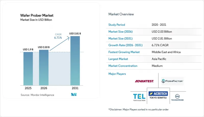
The wafer prober market size in 2026 is estimated at USD 2.03 billion, growing from 2025 value of USD 1.90 billion with 2031 projections showing USD 2.81 billion, growing at 6.71% CAGR over 2026-2031.
This solid growth links directly to the semiconductor sector's rising production capacity and the need to validate ever-smaller, higher-performance chips before packaging. High-volume adoption of advanced packaging, the surge in AI and 5G device output, and the transition to larger wafer formats each reinforce demand for next-generation wafer probers. Vendors are responding by embedding AI in fault detection, integrating predictive maintenance, and improving probe-card precision to keep throughput high and test costs low. The fully automatic segment leads with a 64.1% wafer prober market share in 2024, aided by factory-wide automation programs that target lights-out manufacturing. Contact-based probers still dominate day-to-day test floors, holding 87.2% share, yet non-contact RF solutions are scaling fast to support sub-THz devices.
Global Wafer Prober Market Trends and Insights
3-D IC and Advanced Packaging Boom
Widespread adoption of chiplet architectures and heterogeneous integration is reshaping test requirements. Multidie stacking introduces dense vertical interconnects and new reliability checkpoints that traditional wafer prober designs cannot wholly address. Probe-card suppliers now deploy high-pin-count MEMS arrays that reach thousands of contacts per touchdown to cover large interposer surfaces. FormFactor's custom cards for advanced packages illustrate how simultaneous testing of multiple dies cuts test time while safeguarding signal integrity. The wafer prober market is thus pivoting to high-density, thermally controlled platens capable of +- 50 mK stability, ensuring consistent measurements for power-hungry AI accelerators.
AI / 5G Device Volume Upswing
The explosion of AI processors and 5G chipsets pressures fabs to test far more devices per hour without sacrificing margin. Modern AI SOCs integrate high-bandwidth memory stacks that push probe pads to the edge of the die and demand 50 µm pitch uniformity. Fully automatic probers that self-calibrate alignment in under 2 s per wafer are now central to mass-production lines. Semiconductor Engineering notes that AI-centric testing requires parallelism at the probe card, handler, and ATE levels, a paradigm that raises both current draw and data-logging complexity. Suppliers are adding machine-learning-based scheduling to route wafers to the least congested probers, maximizing overall equipment effectiveness.
High Cap-ex and Long Pay-back
Next-generation fully automatic probers routinely cross USD 3 million per unit, straining cash flow among smaller fabs. Equipment depreciation timelines have stretched as node complexity forces parallel investments in probe cards and data-analytic platforms. EPD Tech calculates that sub-7 nm production costs have topped USD 1 billion, extending ROI horizons beyond 24 months. The wafer prober market thus witnesses deferred purchases or lease models where manufacturers pay by the tested wafer, shifting cap-ex to op-ex.
Other drivers and restraints analyzed in the detailed report include:
- Migration to 200- and 300 mm Fabs
- SiC / GaN Power-Device Ramp-up
- Rising Test-Time per Advanced Node
For complete list of drivers and restraints, kindly check the Table Of Contents.
Segment Analysis
The fully automatic class held a commanding 63.52% wafer prober market share in 2025 and is forecast to post a 8.91% CAGR. Vendors embed robotic wafer loaders, vision-guided alignment, and SECS/GEM interfaces that connect seamlessly with fab MES systems. The SEMISHARE A12 station, recipient of SEMICON China's product innovation award, illustrates step-size accuracy below 1 µm across WAT, CP, and RF sweeps. Labor-light fabs in Korea and Taiwan schedule fleet operation around the clock, lifting utilization rates above 90%.
Semi-automatic units retain a foothold in mid-volume product lines where cycle time is less critical, but flexibility is prized. Manual probes, though small in shipment volume, remain staples in university labs and early device characterization, where quick pad access outweighs automatic wafer exchange speeds.
Contact-based probing still captured 86.55% of 2025 revenue thanks to mature probe-card ecosystems and proven electrical performance. Yet non-contact methods posted a 13.56% CAGR and are now the hottest R&D focus. An IEEE Transactions study described dielectric waveguide couplers that deliver continuous 0 Hz-340 GHz coverage without physical pins. RF-over-air systems avoid probe-mark damage and enable higher reprobing cycles, a major plus for fragile compound-semiconductor wafers.
Probe-card leaders respond with hybrid offerings: vertical MEMS springs for power rails and contactless couplers for millimeter-wave nets on the same card. As 6G prototypes move above 100 GHz, the wafer prober market sees pilot cells that perform DC parametrics and far-field radiation sweeps in a single touchdown.
Wafer Prober Market is Segmented by Product Type (Manual, Semi-Automatic, and Fully Automatic), Technology (Contact, and Non-Contact), Application (Wafer Sort / CP, Package-Level Final Test, and R&D / Failure Analysis), Wafer Size (<=150 Mm, 150-200 Mm, 200-300 Mm, and More), End-User (Foundries, Idms, Osats, and Research and Academia), and Geography (North America, South America, Europe, Asia-Pacific, and Middle East and Africa).
Geography Analysis
Asia-Pacific held 47.05% of the wafer prober market size in 2025, powered by the dense fab clusters of Taiwan, South Korea, and mainland China. TSMC alone reported 74% of Q4 2024 revenue from 7 nm and finer geometries, reinforcing the regional tilt toward cutting-edge nodes. Regional governments offer tax holidays and electricity subsidies that encourage further capacity builds, while domestic probe-card vendors shorten supply lead times.
The Middle East and Africa show the fastest trajectory at an 11.24% CAGR, with Saudi Arabia's USD 100 billion Alat initiative targeting at least 50 design houses by 2030. The UAE courts are founded with free-zone incentives, and reports suggest TSMC is evaluating a UAE site that mirrors its Arizona model. Local demand for AI and defense chips translates into greenfield labs equipped with mid-range probers optimized for 200 mm startup lines.
North America benefits from the USD 52.7 billion CHIPS Act and a pipeline of 300 mm-focused R&D centers. The Arizona State University Research Park will host a flagship testbed for front-end manufacturing and advanced packaging. Europe pursues autonomy via the European Chips Act, allocating grants that modernize probe capacity in Germany, France, and Ireland. Collectively, these initiatives aim to curb reliance on Asian imports and diversify the wafer prober market's revenue base.
- Tokyo Electron Ltd
- Advantest Corp
- FormFactor Inc
- SemiShare Co Ltd
- Micronics Japan Co Ltd
- Accretech (Tokyo Seimitsu)
- MPI Corp
- Wentworth Laboratories Inc
- Technoprobe S.p.A.
- TSE Co Ltd
- Semics Inc
- EverBeing Int'l Corp
- Signatone Corp
- MicroXact Inc
- SEMICAPS Pte Ltd
- Feinmetall GmbH
- INGUN Prufmittelbau GmbH
- SV Probe Pte Ltd
- Chunghwa Precision Test Tech
- Suragus GmbH
- Wuxi Junr Technology Co., Ltd. (JUNR)
- China Micro Semicon Equip (CSEM)
- Signatone Corp
- Tipronics Co Ltd
- STAr Technologies Inc.
- Shibasoku Co Ltd
Additional Benefits:
- The market estimate (ME) sheet in Excel format
- 3 months of analyst support
TABLE OF CONTENTS
1 INTRODUCTION
- 1.1 Study Assumptions and Market Definition
- 1.2 Scope of the Study
2 RESEARCH METHODOLOGY
3 EXECUTIVE SUMMARY
4 MARKET LANDSCAPE
- 4.1 Market Overview
- 4.2 Market Drivers
- 4.2.1 3-D IC and Advanced Packaging Boom
- 4.2.2 AI / 5 G Device Volume Upswing
- 4.2.3 Migration to 200- and 300-mm Fabs
- 4.2.4 SiC / GaN Power-Device Ramp-up
- 4.2.5 National Chip-Fab Subsidies (US/EU)
- 4.2.6 MEMS Micro-probe Array Adoption
- 4.3 Market Restraints
- 4.3.1 High Cap-ex and Long Pay-back
- 4.3.2 Rising Test-time per Advanced Node
- 4.3.3 Precision Probe-Card Supply Bottlenecks
- 4.3.4 In-situ Litho-Stage Test Alternatives
- 4.4 Value Chain Analysis
- 4.5 Regulatory Landscape
- 4.6 Technological Outlook
- 4.7 Porter's Five Forces Analysis
- 4.7.1 Bargaining Power of Suppliers
- 4.7.2 Bargaining Power of Buyers
- 4.7.3 Threat of New Entrants
- 4.7.4 Threat of Substitutes
- 4.7.5 Competitive Rivalry
- 4.8 Impact of Macroeconomic Factors
5 MARKET SIZE AND GROWTH FORECASTS (VALUE)
- 5.1 By Product Type
- 5.1.1 Manual
- 5.1.2 Semi-Automatic
- 5.1.3 Fully Automatic
- 5.2 By Technology
- 5.2.1 Contact
- 5.2.2 Non-contact / RF-over-Air
- 5.3 By Application
- 5.3.1 Wafer Sort / CP
- 5.3.2 Package-Level Final Test
- 5.3.3 R&D / Failure Analysis
- 5.4 By Wafer Size
- 5.4.1 <=150 mm
- 5.4.2 150-200 mm
- 5.4.3 200-300 mm
- 5.4.4 >300 mm (450 mm, Panel)
- 5.5 By End-user
- 5.5.1 Foundries
- 5.5.2 IDMs
- 5.5.3 OSATs
- 5.5.4 Research and Academia
- 5.6 By Geography
- 5.6.1 North America
- 5.6.1.1 United States
- 5.6.1.2 Canada
- 5.6.1.3 Mexico
- 5.6.2 South America
- 5.6.2.1 Brazil
- 5.6.2.2 Argentina
- 5.6.2.3 Rest of South America
- 5.6.3 Europe
- 5.6.3.1 Germany
- 5.6.3.2 United Kingdom
- 5.6.3.3 France
- 5.6.3.4 Italy
- 5.6.3.5 Spain
- 5.6.3.6 Russia
- 5.6.3.7 Rest of Europe
- 5.6.4 Asia-Pacific
- 5.6.4.1 China
- 5.6.4.2 Japan
- 5.6.4.3 India
- 5.6.4.4 South Korea
- 5.6.4.5 South-East Asia
- 5.6.4.6 Rest of Asia-Pacific
- 5.6.5 Middle East and Africa
- 5.6.5.1 Middle East
- 5.6.5.1.1 Saudi Arabia
- 5.6.5.1.2 United Arab Emirates
- 5.6.5.1.3 Turkey
- 5.6.5.1.4 Rest of Middle East
- 5.6.5.2 Africa
- 5.6.5.2.1 South Africa
- 5.6.5.2.2 Nigeria
- 5.6.5.2.3 Rest of Africa
- 5.6.5.1 Middle East
- 5.6.1 North America
6 COMPETITIVE LANDSCAPE
- 6.1 Market Concentration
- 6.2 Strategic Moves
- 6.3 Market Share Analysis
- 6.4 Company Profiles (includes Global-level Overview, Market-level Overview, Core Segments, Financials, Strategic Info, Market Rank/Share, Products and Services, Recent Developments)
- 6.4.1 Tokyo Electron Ltd
- 6.4.2 Advantest Corp
- 6.4.3 FormFactor Inc
- 6.4.4 SemiShare Co Ltd
- 6.4.5 Micronics Japan Co Ltd
- 6.4.6 Accretech (Tokyo Seimitsu)
- 6.4.7 MPI Corp
- 6.4.8 Wentworth Laboratories Inc
- 6.4.9 Technoprobe S.p.A.
- 6.4.10 TSE Co Ltd
- 6.4.11 Semics Inc
- 6.4.12 EverBeing Int'l Corp
- 6.4.13 Signatone Corp
- 6.4.14 MicroXact Inc
- 6.4.15 SEMICAPS Pte Ltd
- 6.4.16 Feinmetall GmbH
- 6.4.17 INGUN Prufmittelbau GmbH
- 6.4.18 SV Probe Pte Ltd
- 6.4.19 Chunghwa Precision Test Tech
- 6.4.20 Suragus GmbH
- 6.4.21 Wuxi Junr Technology Co., Ltd. (JUNR)
- 6.4.22 China Micro Semicon Equip (CSEM)
- 6.4.23 Signatone Corp
- 6.4.24 Tipronics Co Ltd
- 6.4.25 STAr Technologies Inc.
- 6.4.26 Shibasoku Co Ltd
7 MARKET OPPORTUNITIES AND FUTURE OUTLOOK
- 7.1 White-space and Unmet-need Assessment

