PUBLISHER: Mordor Intelligence | PRODUCT CODE: 2044005

PUBLISHER: Mordor Intelligence | PRODUCT CODE: 2044005
Automotive Semiconductor Silicon Wafer - Market Share Analysis, Industry Trends & Statistics, Growth Forecasts (2026 - 2031)
The automotive semiconductor silicon wafer market size is expected to increase from 2.61 Billion Square Inches in 2025 to 2.78 billion Square Inches in 2026 and reach 3.88 Billion Square Inches by 2031, growing at a CAGR of 6.92% over 2026-2031.
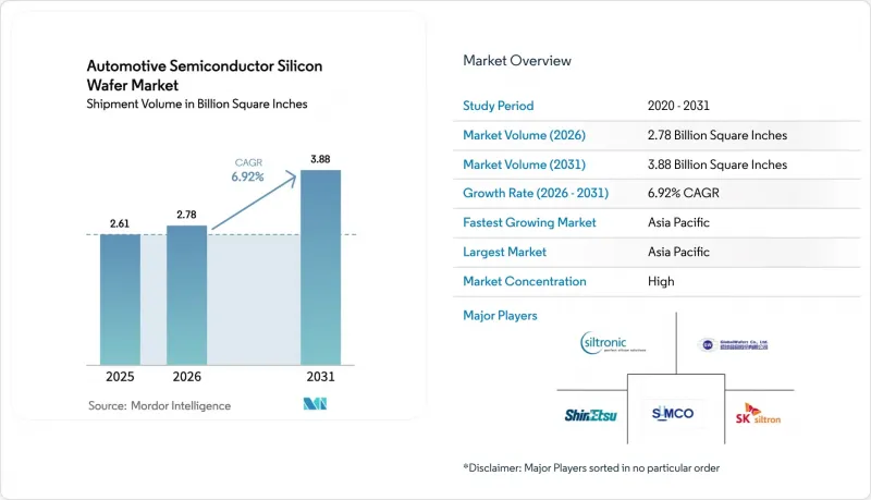
The expansion is powered by the rapid electrification of passenger vehicles, the migration to 800-volt battery packs, and the rise of software-defined vehicle compute domains. Wide-bandgap SiC epitaxial wafers on 200 mm substrates are absorbing much of the incremental volume, even as prime-polished silicon continues to ship the most pieces. Policy incentives in the United States, Europe, South Korea, and India are shortening fab paybacks, while ongoing substrate shortages and long automotive-grade qualification cycles moderate near-term output. Competitive moves toward vertical integration and 300 mm migration are reshaping cost curves and will decide the future trajectory of the automotive semiconductor silicon wafer market.
Global Automotive Semiconductor Silicon Wafer Market Trends and Insights
Rising EV Penetration And Shift Toward 800V Vehicle Platforms
Electric models built on 800-volt packs need SiC MOSFETs rated at 1,200 V, which in turn require 200 mm epitaxial wafers with extremely low basal-plane dislocation densities. Launches such as Hyundai's Ioniq 5 and Kia's EV6 have triggered similar roadmaps from Porsche, Audi, and General Motors for model-year 2026 designs. Capacity additions at Infineon's Kulim facility and long-term wafer supply agreements signed by STMicroelectronics underscore the race to lock in material ahead of volume hikes. The structural pull tightens lead times beyond 12 months and underscores the importance of secure substrate access.
Rapid Build-Out Of 800V Charging Infrastructure
Public and private spending on ultra-fast charging surpassed USD 12 billion in 2025, and Europe's AFIR rule mandates 400 kW chargers every 60 km on core corridors by 2027. Each 800 V on-board charger integrates six to eight SiC MOSFETs grown on 150 mm- to 200-mm wafers, so faster charger rollouts translate directly into increased wafer demand. Chinese deployments already account for more than 60% of global 800 V posts, reinforcing Asia-Pacific's dominance. Soitec's Power-SOI substrates are winning gate-driver sockets where PCB area is tight. Because OBC design cycles lag infrastructure by roughly 18 months, the full volume effect will surface between 2027 and 2028.
Limited Availability Of 200 mm Substrates
Global capacity reached only 1.2 million 200 mm SiC wafers in 2025, yet automotive demand will surpass 2 million units before 2028. Each PVT reactor costs up to USD 8 million and needs 18-24 months to qualify, delaying meaningful relief. Wolfspeed's Siler City expansion runs through 2027, while European and North American OEMs still rely heavily on Asian imports. The shortage forces dual-sourcing and stretches design cycles, trimming 1.2 percentage points off the sector CAGR in the near term.
Other drivers and restraints analyzed in the detailed report include:
- High-Temperature, High-Frequency Performance Advantages Over Si
- Government Incentives For Wide-Band-Gap Fabs
- Packaging-Induced Thermo-Mechanical Stress
For complete list of drivers and restraints, kindly check the Table Of Contents.
Segment Analysis
The 200 mm tranche held 56.48% automotive semiconductor silicon wafer market share in 2025 and remains indispensable for SiC power discretes, gate drivers, and PMICs. Mature-node lines already depreciated keep operating margins attractive, and the die sizes of traction MOSFETs fit 200 mm economics well. However, 300 mm capacity is climbing at a 7.45% CAGR because Texas Instruments, TSMC, and GlobalWafers are shifting MCUs and mixed-signal ICs onto larger wafers, driving 20%-plus cost reductions per die. Wolfspeed's 300 mm SiC samples delivered sub-1 cm-2 defect densities, proving technical feasibility and pointing toward high-volume power-device supply after 2028.
The automotive semiconductor silicon wafer market is likely to bifurcate, 300 mm will dominate compute and mixed-signal content once qualification barriers fall, while 200 mm persists in SiC until crystal growth catches up. Up-to-150 mm formats continue sliding as legacy fabs retire, although they retain pockets of demand for thyristors and custom analog. Soitec is migrating Power-SOI to 300 mm to meet demand for battery management, highlighting the need for tighter cost structures in electrification programs.
The Automotive Semiconductor Silicon Wafer Market Report is Segmented by Wafer Diameter (Up To 150 Mm, 200 Mm, and 300 Mm), Semiconductor Device Type (Logic, Memory, Analog, Discrete, and Other Types), Wafer Type (Prime Polished, Epitaxial, SOI, and Specialty Silicon), and Geography (North America, Europe, Asia-Pacific, South America, Middle East and Africa). The Market Forecasts are Provided in Terms of Volume (Square Inches).
Geography Analysis
Asia-Pacific held 84.19% automotive semiconductor silicon wafer market share in 2025 and is expanding at 7.59% CAGR. Taiwan accounts for a considerable share of sub-6 nm capacity and more than 40% of mature-node automotive wafer starts, while China continues to integrate SiC crystal growth, epitaxy, and device fabs. South Korea's 700 trillion KRW (USD 525 billion) strategy adds 10 new facilities and compound-semiconductor lines, reinforcing regional depth. Japan's substrate majors, including Shin-Etsu and SUMCO, anchor 300 mm prime polished and SiC epitaxial supply, and India's state-backed 12-inch line will bring 50,000 wafers per month online in 2026.
North America controlled a small share of shipments in 2025, but CHIPS Act incentives fund GlobalWafers' 300 mm plant and Wolfspeed's SiC megafab, together adding more than one million 200 mm-equivalent wafers annually by 2028. The localization push, however, still leaves many modules reliant on Asian substrates, as U.S. light-vehicle output surpasses 15 million units yearly. Europe holds a considerable share and benefits from IPCEI-ME/CT funding for capacity at Infineon, STMicroelectronics, and GlobalWafers, yet imports cover over 70% of prime polished demand.
South America plus Middle East and Africa together remain low due to limited ecosystem depth and capital barriers. To mitigate supply-chain risk, automakers now co-qualify multiple geographic sources even though the 18-to-24-month automotive-grade cycle delays meaningful diversification until late 2027. Inventory corrections that began in late-2024 appear to have bottomed by early-2026, and wafer call-offs are rebounding under new long-term supply agreements.
- Shin-Etsu Chemical Co., Ltd.
- SUMCO Corporation
- Siltronic AG
- GlobalWafers Co., Ltd.
- SK Siltron Co., Ltd.
- Soitec S.A.
- Okmetic Oy
- Wafer Works Corp.
- Topsil Semiconductor Materials A/S
- Shanghai Simgui Technology Co., Ltd.
- MEMC Electronic Materials, Inc.
- Infineon Technologies AG
- ON Semiconductor Corp.
- STMicroelectronics N.V.
- NXP Semiconductors N.V.
- Renesas Electronics Corp.
- Texas Instruments Inc.
- X-FAB Silicon Foundries SE
- Wolfspeed, Inc.
Additional Benefits:
- The market estimate (ME) sheet in Excel format
- 3 months of analyst support
TABLE OF CONTENTS
1 INTRODUCTION
- 1.1 Study Assumptions and Market Definition
- 1.2 Scope of the Study
2 RESEARCH METHODOLOGY
3 EXECUTIVE SUMMARY
4 MARKET LANDSCAPE
- 4.1 Market Overview
- 4.2 Industry Value Chain Analysis
- 4.3 Technology Analysis
- 4.4 Impact of Macroeconomic Factors on the Market
- 4.5 Porter's Five Forces Analysis
- 4.5.1 Bargaining Power of Suppliers
- 4.5.2 Bargaining Power of Buyers
- 4.5.3 Threat of New Entrants
- 4.5.4 Threat of Substitutes
- 4.5.5 Intensity of Competitive Rivalry
- 4.6 Market Drivers
- 4.6.1 Rising EV Penetration and Shift Toward 800-V Vehicle Platforms
- 4.6.2 Rapid Build-Out of 800 V Charging Infrastructure
- 4.6.3 High-Temperature, High-Frequency Performance Advantages Over Si
- 4.6.4 Government Incentives for Wide-Band-Gap Fabs
- 4.6.5 Emergence of Vertically-Integrated SiC Supply Chains in China
- 4.6.6 Novel 200 mm Bulk-Growth Breakthroughs Lowering Defect Density
- 4.7 Market Restraints
- 4.7.1 Limited Availability of 200 mm Substrates
- 4.7.2 Packaging-Induced Thermo-Mechanical Stress
- 4.7.3 Capital-Intensive Crystal-Growth Equipment
- 4.7.4 Recycling Challenges for SiC Kerf Waste
5 MARKET SIZE AND GROWTH FORECASTS (VOLUME)
- 5.1 By Wafer Diameter
- 5.1.1 Up to 150 mm
- 5.1.2 200 mm
- 5.1.3 300 mm
- 5.2 By Semiconductor Device Type
- 5.2.1 Logic
- 5.2.2 Memory
- 5.2.3 Analog
- 5.2.4 Discrete
- 5.2.5 Other Semiconductor Device Types
- 5.3 By Wafer Type
- 5.3.1 Prime Polished
- 5.3.2 Epitaxial
- 5.3.3 Silicon-on-Insulator (SOI)
- 5.3.4 Specialty Silicon (High-Resistivity, Power, Sensor-Grade)
- 5.4 By Geography
- 5.4.1 North America
- 5.4.1.1 United States
- 5.4.1.2 Canada
- 5.4.1.3 Mexico
- 5.4.2 Europe
- 5.4.2.1 Germany
- 5.4.2.2 United Kingdom
- 5.4.2.3 France
- 5.4.2.4 Rest of Europe
- 5.4.3 Asia-Pacific
- 5.4.3.1 China
- 5.4.3.2 Japan
- 5.4.3.3 India
- 5.4.3.4 South Korea
- 5.4.3.5 Taiwan
- 5.4.3.6 Rest of Asia-Pacific
- 5.4.4 South America
- 5.4.5 Middle East and Africa
- 5.4.1 North America
6 COMPETITIVE LANDSCAPE
- 6.1 Market Concentration
- 6.2 Strategic Moves
- 6.3 Market Share Analysis
- 6.4 Company Profiles (includes Global Level Overview, Market Level Overview, Core Segments, Financials as available, Strategic Information, Market Rank/Share, Products and Services, Recent Developments)
- 6.4.1 Shin-Etsu Chemical Co., Ltd.
- 6.4.2 SUMCO Corporation
- 6.4.3 Siltronic AG
- 6.4.4 GlobalWafers Co., Ltd.
- 6.4.5 SK Siltron Co., Ltd.
- 6.4.6 Soitec S.A.
- 6.4.7 Okmetic Oy
- 6.4.8 Wafer Works Corp.
- 6.4.9 Topsil Semiconductor Materials A/S
- 6.4.10 Shanghai Simgui Technology Co., Ltd.
- 6.4.11 MEMC Electronic Materials, Inc.
- 6.4.12 Infineon Technologies AG
- 6.4.13 ON Semiconductor Corp.
- 6.4.14 STMicroelectronics N.V.
- 6.4.15 NXP Semiconductors N.V.
- 6.4.16 Renesas Electronics Corp.
- 6.4.17 Texas Instruments Inc.
- 6.4.18 X-FAB Silicon Foundries SE
- 6.4.19 Wolfspeed, Inc.
7 MARKET OPPORTUNITIES AND FUTURE OUTLOOK
- 7.1 White-Space and Unmet-Need Assessment

