
PUBLISHER: Mordor Intelligence | PRODUCT CODE: 2044172

PUBLISHER: Mordor Intelligence | PRODUCT CODE: 2044172
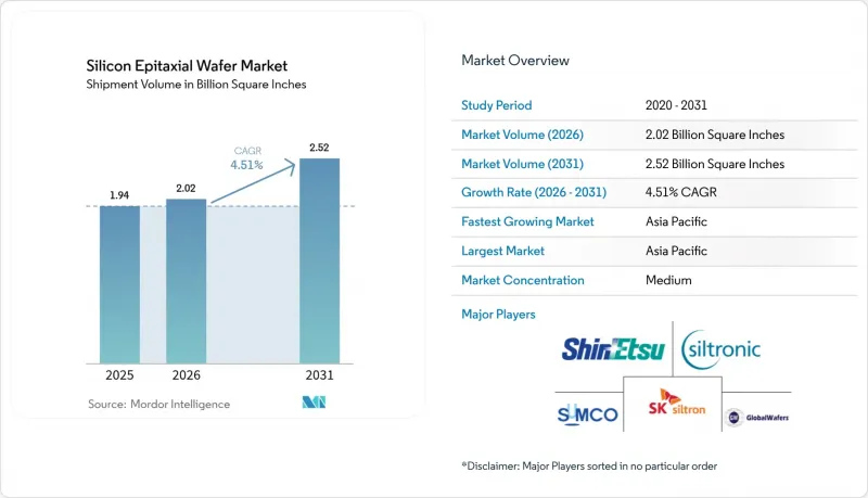
Silicon Epitaxial Wafer - Market Share Analysis, Industry Trends & Statistics, Growth Forecasts (2026 - 2031)
The epitaxial silicon wafer market size is projected to expand from 1,938.59 million square inches in 2025, 2,018.27 million square inches in 2026, to 2,516.09 million square inches by 2031, registering a 4.51% CAGR over 2026-2031.
Thicker, ultra-low-defect layers for 300 mm substrates, backside-power-delivery adoption, and rising demand from automotive electrification and on-device AI inference together underpin a durable volume floor. Asia-Pacific's installed reactor base, government subsidies, and memory-capability additions keep regional output dominant, while quantum-computing prototypes on isotopically purified Si-28 layers point to a strategically important future niche. Capital expenditure above USD 120 million for an eight-reactor 300 mm line, coupled with volatile polysilicon feedstock pricing, pushes smaller suppliers to exit or consolidate. Incumbents are moving to renewable-powered cleanrooms and lower-temperature selective-epitaxy modules to satisfy carbon-footprint scrutiny and lithography overlay budgets below 1.5 nm.
Global Silicon Epitaxial Wafer Market Trends and Insights
Rising Demand for 300 mm Logic and Memory Capacity Expansions
Foundries and integrated device makers pledged USD 165 billion to new 300 mm fabs during 2025-2026, including TSMC's Phoenix megafab, Samsung's Taylor facility, and SK Hynix's P&T7 plant. Together, these sites will require more than 50 million square inches of epitaxial wafers annually by 2028, and each 2 nm or 3 nm logic wafer needs a rigorously tuned layer to control threshold-voltage spread. Memory producers are stretching high-bandwidth-memory stacks to 12-16 layers, demanding thinner base wafers with engineered stress to avoid warpage in through-silicon-via drilling. The combined logic-memory pipeline stabilizes baseline demand and shields suppliers from the polished-wafer boom-bust pattern. Intel and TSMC's backside-power-delivery roadmaps further compress tolerance to +-1% across a 300 mm-diameter.
Semiconductor Device Scaling Driving Demand for Ultra-Low-Defect Density Epi Wafers
Gate-all-around transistors debuting at 3 nm and maturing at 2 nm cut the allowable defect density to below 0.01 cm-2, a tenfold tightening compared to fin-FETs. Vertical nanosheet stacks amplify the damage caused by single dislocations, reducing drive current by up to 15%. Suppliers now pair in-situ hydrogen anneals with ultra-high-purity precursors, raising capital intensity but enabling node transitions. Reducing design rules for power and ground rails magnifies the penalty for epi-induced stress during extreme-ultraviolet exposure. The economic split pushes premium ultra-low-defect products to command 30-50% price premiums as stickier, longer contracts emerge.
Escalating Capex for 300 mm Epitaxy Reactors and Automation
A single 300 mm CVD reactor costs USD 12-15 million, and a greenfield line requires 8-12 reactors, plus USD 30-50 million in automation, bringing upfront investment to roughly USD 150-170 million before cleanroom fit-out. Smaller producers struggle to amortize that load, as Siltronic's July 2025 exit from 150 mm production showed. In 2024-2025, rising interest rates led to an increase in the weighted-average cost of capital. This shift resulted in delays for certain expansions and favored established players who could leverage their balance-sheet cash.
Other drivers and restraints analyzed in the detailed report include:
- Surge in Automotive ADAS and Power Electronics Requiring High-Quality Epi Layers
- Government Subsidies for Domestic 300 mm Wafer Fabs in Asia-Pacific
- Volatile Silicon Feedstock Prices Compressing Wafer Margins
For complete list of drivers and restraints, kindly check the Table Of Contents.
Segment Analysis
The 300 mm class delivered 68.49% of shipments in 2025, reflecting its centrality to leading-edge nodes and setting the baseline for the epitaxial silicon wafer market size. Backside power delivery lifts layer thickness by 15-20%, driving higher reactor utilization at Shin-Etsu and SUMCO. SEMI tightened flatness and bow limits by 30% since 2023, compelling suppliers to upgrade metrology and process control. Conversely, a retrofit wave in older fabs keeps 200 mm demand expanding at a 4.95% CAGR, defying earlier forecasts of terminal decline. Okmetic's EUR 400 million (USD 452 million) Vantaa expansion, operational in 2026, doubled 200 mm capacity to serve automotive sensors and mixed-signal ICs, while Wafer Works and Episil also grew 200 mm output. The 150 mm and smaller pool is shrinking, yet niche optoelectronics players retain specialized capacity.
200 mm momentum is heavily automotive-driven, as power-module makers retrofit lines for silicon-carbide gate drivers and ADAS sensor ICs. China's push for self-sufficiency in mature-node technology further elevates 200 mm volumes. Meanwhile, 300 mm investments stay concentrated in Asia-Pacific, cementing the region's dominance in the epitaxial silicon wafer market.
The Silicon Epitaxial Wafer Market Report is Segmented by Wafer Diameter (Up To 150 Mm, 200 Mm, and More), Semiconductor Device Type (Logic, Memory, and More), End-User Industry (Consumer Electronics, Automotive, Industrial, and More), and Geography. The Market Forecasts are Provided in Terms of Volume (Square Inches).
Geography Analysis
Asia-Pacific commanded 80.41% of 2025 volume and is projected to expand at a 5.58% CAGR through 2031. Taiwan leads advanced-logic output, South Korea dominates memory, and China's self-reliance plan increases mature-node pulls, together underpinning the region's share of the epitaxial silicon wafer market size. Japan's USD 6.8 billion incentive package for TSMC Kumamoto and Rapidus ensures local supply continuity, while China's export-control risks spur stockpiling by domestic fabs. India's Gujarat project adds a future foothold, though initial wafers will be imported.
North America held a mid-single-digit slice in 2025 but benefits from the CHIPS and Science Act grants. GlobalWafers' Sherman plant, opened in May 2025, and Intel's Ohio megafab will together demand more than 10 million square inches a year by 2028. Europe lags on cost and permitting, yet Siltronic's Singapore 300 mm line and GlobalWafers' Novara, Italy site, opened in October 2025 with EUR 400 million (USD 452 million) in subsidies, secure automotive-focused supply routes. South America, along with the Middle East and Africa, remains import-dependent, with limited near-term prospects for indigenous capacity.
Regional concentration raises strategic-dependency alarms in the United States and Europe, prompting subsidy races and export controls. Still, Asia-Pacific's reactor installed base, process know-how, and cluster economics make its dominance in the epitaxial silicon wafer market difficult to dislodge before the next decade.
- Shin-Etsu Handotai Co. Ltd.
- SUMCO Corporation
- GlobalWafers Co. Ltd.
- Siltronic AG
- SK Siltron Co. Ltd.
- Okmetic Oyj
- Wafer Works Corporation
- Poshing Silicon Co. Ltd.
- Simgui Shanghai
- Hebei Semiconductor
- Soitec S.A.
- Episil Technologies Inc.
- MCL Electronic Materials Ltd.
- Siltronix Silicon Technologies
- Advanced Micro-Fabrication Equipment Inc.
- Ferrotec Holdings Corporation
- Topco Scientific Co. Ltd.
- Nova Electronic Materials LLC
- Shenhe Thermo-Magnetics Electronics Co.
- Addison Engineering Inc.
- Virginia Semiconductor Inc.
Additional Benefits:
- The market estimate (ME) sheet in Excel format
- 3 months of analyst support
TABLE OF CONTENTS
1 INTRODUCTION
- 1.1 Study Assumptions and Market Definition
- 1.2 Scope of the Study
2 RESEARCH METHODOLOGY
3 EXECUTIVE SUMMARY
4 MARKET LANDSCAPE
- 4.1 Market Overview
- 4.2 Industry Value-Chain Analysis
- 4.3 Regulatory Landscape
- 4.4 Impact of Macroeconomic Factors
- 4.5 Technology Analysis
- 4.6 Porter's Five Forces Analysis
- 4.6.1 Bargaining Power of Suppliers
- 4.6.2 Bargaining Power of Buyers
- 4.6.3 Threat of New Entrants
- 4.6.4 Threat of Substitutes
- 4.6.5 Intensity of Competitive Rivalry
- 4.7 Market Drivers
- 4.7.1 Semiconductor Device Scaling Driving Demand for Ultra-Low Defect Density Epi Wafers
- 4.7.2 Rising Demand for 300 mm Logic and Memory Capacity Expansions
- 4.7.3 Surge in Automotive ADAS and Power Electronics Requiring High-Quality Epi Layers
- 4.7.4 Government Subsidies for Domestic 300 mm Wafer Fabs in Asia-Pacific
- 4.7.5 Adoption of Backside-Power-Delivery Architectures Boosting Epi Thickness Needs
- 4.7.6 Emergence of Quantum-Computing Qubits on Isotopically Purified Si-28 Epi Layers
- 4.8 Market Restraints
- 4.8.1 Escalating Capex for 300 mm Epitaxy Reactors and Automation
- 4.8.2 Volatile Silicon Feedstock Prices Compressing Wafer Margins
- 4.8.3 Lithography-Induced Pattern Collapse from Epi Stress Mismatches
- 4.8.4 Carbon-Footprint Scrutiny of Energy-Intensive CVD Epitaxy Processes
5 MARKET SIZE AND GROWTH FORECASTS (VOLUME)
- 5.1 By Wafer Diameter
- 5.1.1 Up to 150 mm
- 5.1.2 200 mm
- 5.1.3 300 mm
- 5.2 By Semiconductor Device Type
- 5.2.1 Logic
- 5.2.2 Memory
- 5.2.3 Analog
- 5.2.4 Discrete
- 5.2.5 Other Semiconductor Device Types (Optoelectronics, Sensors, Micro)
- 5.3 By End-user
- 5.3.1 Consumer Electronics
- 5.3.1.1 Mobile and Smartphones
- 5.3.1.2 PCs and Servers
- 5.3.2 Industrial
- 5.3.3 Telecommunications
- 5.3.4 Automotive
- 5.3.5 Other End-user Applications
- 5.3.1 Consumer Electronics
- 5.4 By Geography
- 5.4.1 North America
- 5.4.1.1 United States
- 5.4.1.2 Canada
- 5.4.1.3 Mexico
- 5.4.2 Europe
- 5.4.2.1 Germany
- 5.4.2.2 United Kingdom
- 5.4.2.3 France
- 5.4.2.4 Rest of Europe
- 5.4.3 Asia-Pacific
- 5.4.3.1 China
- 5.4.3.2 Japan
- 5.4.3.3 India
- 5.4.3.4 South Korea
- 5.4.3.5 Taiwan
- 5.4.3.6 Rest of Asia-Pacific
- 5.4.4 South America
- 5.4.5 Middle East and Africa
- 5.4.1 North America
6 COMPETITIVE LANDSCAPE
- 6.1 Market Concentration
- 6.2 Strategic Moves
- 6.3 Market Share Analysis
- 6.4 Company Profiles (includes Global Level Overview, Market Level Overview, Core Segments, Financials as available, Strategic Information, Market Rank/Share, Products and Services, Recent Developments)
- 6.4.1 Shin-Etsu Handotai Co. Ltd.
- 6.4.2 SUMCO Corporation
- 6.4.3 GlobalWafers Co. Ltd.
- 6.4.4 Siltronic AG
- 6.4.5 SK Siltron Co. Ltd.
- 6.4.6 Okmetic Oyj
- 6.4.7 Wafer Works Corporation
- 6.4.8 Poshing Silicon Co. Ltd.
- 6.4.9 Simgui Shanghai
- 6.4.10 Hebei Semiconductor
- 6.4.11 Soitec S.A.
- 6.4.12 Episil Technologies Inc.
- 6.4.13 MCL Electronic Materials Ltd.
- 6.4.14 Siltronix Silicon Technologies
- 6.4.15 Advanced Micro-Fabrication Equipment Inc.
- 6.4.16 Ferrotec Holdings Corporation
- 6.4.17 Topco Scientific Co. Ltd.
- 6.4.18 Nova Electronic Materials LLC
- 6.4.19 Shenhe Thermo-Magnetics Electronics Co.
- 6.4.20 Addison Engineering Inc.
- 6.4.21 Virginia Semiconductor Inc.
7 MARKET OPPORTUNITIES AND FUTURE OUTLOOK
- 7.1 White-Space and Unmet-Need Assessment

