
PUBLISHER: Mordor Intelligence | PRODUCT CODE: 2061513

PUBLISHER: Mordor Intelligence | PRODUCT CODE: 2061513
Semiconductor Packaging - Market Share Analysis, Industry Trends & Statistics, Growth Forecasts (2026 - 2031)
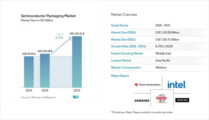
According to Mordor Intelligence, the semiconductor packaging market size is projected to be USD 95.40 billion in 2025, USD 103.08 billion in 2026, and reach USD 156.41 billion by 2031, growing at a CAGR of 8.70% from 2026 to 2031.
This report is Segmented by Packaging Platform (Advanced Packaging, Traditional Packaging), Packaging Material (Organic Substrates, Leadframes, Bonding Wires, and More), Wafer Size (Below 200 Mm, 300 Mm, Above 450 Mm/Panel), Business Model (OSAT, Foundry Back-End, IDM In-House), End-User Industry (Consumer Electronics, and More), and Geography. The Market Forecasts are Provided in Terms of Value (USD).
Global Semiconductor Packaging Market Trends and Insights
AI Accelerator Boom Driving 2.5D/3D Interposers
Hyperscale data-center operators now deploy clusters with more than 30,000 graphics processing units per site, each relying on high-yield interposers to connect logic dies to high-bandwidth memory stacks. Throughout 2025, TSMC reported CoWoS capacity utilization above 95%, prompting customers to secure slots through 2027. At 2.5D geometries, average yield hovers near 75%, meaning one in four substrates is scrapped at a cost that can top USD 10,000 per defect. Intel's Meteor Lake processors, shipped in 2024, demonstrated a 10-micron bump pitch, trimming package area by 40% but pushing thermal density toward 200 W/cm2. Smaller fabless firms without long-term contracts face allocation risk as hyperscalers monopolize supply.
Electrified Vehicle Power Packages in the United States and Asia
Electric-vehicle inverters require power modules that survive junction temperatures above 200 °C and repeated 150 °C thermal cycles. Wolfspeed doubled automotive design wins for 800-volt architectures in fiscal 2025, with each inverter consuming up to 12 discrete modules.[2] Ceramic substrates from Kyocera and NGK Spark Plug exhibit thermal conductivities above 250 W/m*K but cost several times more than organic laminates. Domestic-content incentives in the United States prompted Infineon and ON Semiconductor to commit USD 2 billion in packaging investments across Texas and New York. China's vertically integrated BYD and CATL likewise internalized module assembly to secure performance and margin.
ABF Substrate Supply Crunch (Taiwan/Japan)
Ajinomoto Build-up Film substrates remained in short supply during 2025 because capacity expansions at Ibiden and Shinko Electric will not reach volume until mid-2026. Lead times for 12-layer substrates stretched to 38 weeks, forcing redesigns or performance compromises. One tier-1 cloud provider responded by investing USD 300 million in a Taiwanese joint venture to lock in supply.
Other drivers and restraints analyzed in the detailed report include:
- United States and EU CHIPS Incentives Creating Local Back-End Fabs
- Chiplet Architectures Powering High-Density Interposers
- Yield Challenges in 3D TSV/Hybrid Bonding
For complete list of drivers and restraints, kindly check the Table Of Contents.
Segment Analysis
Advanced formats accounted for 65.71% of the semiconductor packaging market share in 2025 and are set to grow at a 10.61% CAGR through 2031. Flip-chip remains dominant for high-pin-count devices as solder-bump pitch tightens to 80 µm. Fan-out wafer-level packaging delivers 20% savings in bill of materials for 5G RF front-ends, while system-in-package and package-on-package architectures optimize mobile footprints. The 2.5D/3D subsegment is the fastest climber, driven by AI accelerators that embed eight or more high-bandwidth memory stacks per interposer.
Panel-level packaging is emerging as a cost disruptor, expected to expand at a 10.89% CAGR through 2031. Rectangular 510 mm X 515 mm substrates yield 2.5 times as many dies as 300 mm wafers, lowering per-die cost by up to 40%. Yet new handling and inspection tools are required, pushing the learning curve to 24 months. Traditional wire-bond solutions preserve relevance in power management ICs, discrete transistors, and legacy automotive applications where cost and qualification inertia dominate.
Organic laminates held a 37.82% share in 2025, but Ajinomoto Build-up Film's supply constraints prompt design diversification. Leadframes, bonding wires, encapsulation resins, and solder balls collectively support price-sensitive devices. Copper wire adoption reached over 80% by 2025, saving USD 0.02-0.05 per unit compared with gold. Epoxy molding compounds now incorporate silicone variants to tolerate automotive temperatures above 150 °C.
Ceramic packages are forecast to grow at an 11.67% CAGR, driven by silicon-carbide and gallium-nitride power modules that require thermal conductivity above 200 W/m*K. Kyocera's 2024 expansion increased aluminum nitride capacity by 25%. Die attach and thermal interface compounds have become critical as logic power density exceeds 100 W/cm2. The semiconductor packaging market continues to scrutinize second-source options for ABF dielectric to avoid single-supplier risk.
Geography Analysis
Asia-Pacific controlled 66.89% of the semiconductor packaging market in 2025, anchored by Taiwan's leadership in flip-chip and fan-out processing and China's scale in mainstream assembly. Export controls enacted in October 2024 continue to limit mainland access to state-of-the-art tools, prompting domestic players to adopt hybrid-bonding workarounds that sacrifice yield for autonomy. South Korea's Samsung and SK Hynix vertically integrate memory packaging, while Japan's Shinko Electric and Ibiden dominate high-layer-count substrate fabrication.
North America's share is rising as CHIPS Act incentives underwrite new lines in Arizona, New Mexico, Texas, and Ohio. Amkor's USD 2-billion plant in Arizona and Intel's packaging expansions bring advanced capability within the region, supporting defense and automotive security requirements. Europe remains smaller but is set to double capacity by 2030 through the EU Chips Act, with Germany's Dresden cluster leading investment.
The Middle East exhibits the fastest regional CAGR at 11.29% as Saudi Arabia's Public Investment Fund and the United Arab Emirates' Mubadala channel oil revenues into semiconductor diversification. Greenfield assembly and test lines scheduled for 2027-2028 will target consumer and automotive modules before progressing to advanced interposers. South America and Africa maintain niche participation, focusing on wire-bond and leadframe services for localized industrial demand.
- ASE Technology Holding Co., Ltd.
- Amkor Technology, Inc.
- JCET Group Co., Ltd.
- Siliconware Precision Industries Co., Ltd.
- Powertech Technology Inc.
- Tianshui Huatian Technology Co., Ltd.
- UTAC Holdings Ltd.
- ChipMOS Technologies Inc.
- Chipbond Technology Corp.
- Intel Corporation
- Samsung Electronics Co., Ltd.
- Taiwan Semiconductor Manufacturing Co. Ltd.
- Micron Technology, Inc.
- Texas Instruments Inc.
- Advanced Micro Devices, Inc.
- Hana Micron Inc.
- Nepes Corporation
- TongFu Microelectronics Co., Ltd.
- Shinko Electric Industries Co., Ltd.
- Unisem (M) Berhad
Additional Benefits:
- The market estimate (ME) sheet in Excel format
- 3 months of analyst support
TABLE OF CONTENTS
1 INTRODUCTION
- 1.1 Study Assumptions and Market Definition
- 1.2 Scope of the Study
2 RESEARCH METHODOLOGY
3 EXECUTIVE SUMMARY
4 MARKET LANDSCAPE
- 4.1 Market Overview
- 4.2 Market Drivers
- 4.2.1 AI Accelerator Boom Driving 2.5D/3D Interposers
- 4.2.2 Electrified Vehicle Power Packages in United States and Asia
- 4.2.3 US-EU CHIPS Incentives Creating Local Back-End Fabs
- 4.2.4 5G RF-SiP Demand in China and Korea
- 4.2.5 Panel Level Packaging for Ultra-Low-Cost IoT
- 4.2.6 Chiplet Architectures Powering High-Density Interposers
- 4.3 Market Restraints
- 4.3.1 ABF Substrate Supply Crunch (Taiwan/Japan)
- 4.3.2 Yield Challenges in 3D TSV/Hybrid Bonding
- 4.3.3 Export Controls on Advanced Packaging Tools to China
- 4.3.4 Thermal Dissipation Limits in Fan-Out WLP at below 5 nm
- 4.4 Industry Value Chain Analysis
- 4.5 Regulatory Outlook
- 4.6 Impact of Macroeconomic Factors on the Market
- 4.7 Technological Outlook
- 4.8 Porter's Five Forces Analysis
- 4.8.1 Bargaining Power of Suppliers
- 4.8.2 Bargaining Power of Buyers
- 4.8.3 Threat of New Entrants
- 4.8.4 Threat of Substitutes
- 4.8.5 Intensity of Competitive Rivalry
- 4.9 Industry Capacity and Investment Trend Analysis
- 4.10 Pricing Analysis
5 MARKET SIZE AND GROWTH FORECASTS (VALUE)
- 5.1 By Packaging Platform
- 5.1.1 Advanced Packaging
- 5.1.1.1 Flip-Chip
- 5.1.1.2 Fan-Out WLP
- 5.1.1.3 Fan-In WLP
- 5.1.1.4 2.5D / 3D IC
- 5.1.1.5 Embedded-Die
- 5.1.1.6 SiP / PoP
- 5.1.1.7 Panel-Level Packaging
- 5.1.2 Traditional Packaging
- 5.1.2.1 Wire-Bond
- 5.1.2.2 Leadframe
- 5.1.2.3 QFN / QFP / SOP
- 5.1.1 Advanced Packaging
- 5.2 By Packaging Material
- 5.2.1 Organic Substrates
- 5.2.2 Leadframes
- 5.2.3 Bonding Wires
- 5.2.4 Encapsulation Resins
- 5.2.5 Ceramic Packages
- 5.2.6 Solder Balls and Bumps
- 5.2.7 Die-Attach and TIMs
- 5.3 By Wafer Size
- 5.3.1 Below 200 mm
- 5.3.2 300 mm
- 5.3.3 Above 450 mm / Panel
- 5.4 By Business Model
- 5.4.1 OSAT
- 5.4.2 Foundry Back-End
- 5.4.3 IDM In-house
- 5.5 By End-user Industry
- 5.5.1 Consumer Electronics
- 5.5.1.1 Smartphones and Wearables
- 5.5.1.2 PCs, Tablets, and Consumer Devices
- 5.5.2 Computing and Data Center
- 5.5.3 Automotive and Mobility
- 5.5.4 Communications and Telecom
- 5.5.5 Aerospace and Defense
- 5.5.6 Medical and Healthcare Devices
- 5.5.7 Industrial and Energy (LED / Power)
- 5.5.1 Consumer Electronics
- 5.6 By Geography
- 5.6.1 North America
- 5.6.1.1 United States
- 5.6.1.2 Canada
- 5.6.1.3 Mexico
- 5.6.2 Europe
- 5.6.2.1 Germany
- 5.6.2.2 United Kingdom
- 5.6.2.3 France
- 5.6.2.4 Rest of Europe
- 5.6.3 Asia-Pacific
- 5.6.3.1 China
- 5.6.3.2 Japan
- 5.6.3.3 India
- 5.6.3.4 South Korea
- 5.6.3.5 Taiwan
- 5.6.3.6 Rest of Asia-Pacific
- 5.6.4 Rest of the World
- 5.6.1 North America
6 COMPETITIVE LANDSCAPE
- 6.1 Market Concentration
- 6.2 Strategic Moves
- 6.3 Market Share Analysis
- 6.4 Company Profiles (includes Global Level Overview, Market Level Overview, Core Segments, Financials as Available, Strategic Information, Market Rank/Share, Products and Services, Recent Developments)
- 6.4.1 ASE Technology Holding Co., Ltd.
- 6.4.2 Amkor Technology, Inc.
- 6.4.3 JCET Group Co., Ltd.
- 6.4.4 Siliconware Precision Industries Co., Ltd.
- 6.4.5 Powertech Technology Inc.
- 6.4.6 Tianshui Huatian Technology Co., Ltd.
- 6.4.7 UTAC Holdings Ltd.
- 6.4.8 ChipMOS Technologies Inc.
- 6.4.9 Chipbond Technology Corp.
- 6.4.10 Intel Corporation
- 6.4.11 Samsung Electronics Co., Ltd.
- 6.4.12 Taiwan Semiconductor Manufacturing Co. Ltd.
- 6.4.13 Micron Technology, Inc.
- 6.4.14 Texas Instruments Inc.
- 6.4.15 Advanced Micro Devices, Inc.
- 6.4.16 Hana Micron Inc.
- 6.4.17 Nepes Corporation
- 6.4.18 TongFu Microelectronics Co., Ltd.
- 6.4.19 Shinko Electric Industries Co., Ltd.
- 6.4.20 Unisem (M) Berhad
7 MARKET OPPORTUNITIES AND FUTURE OUTLOOK
- 7.1 White-Space and Unmet-Need Assessment

