
PUBLISHER: Mordor Intelligence | PRODUCT CODE: 2065428

PUBLISHER: Mordor Intelligence | PRODUCT CODE: 2065428
Through-Silicon Via (TSV) For GPU And AI Accelerators - Market Share Analysis, Industry Trends & Statistics, Growth Forecasts (2026 - 2031)
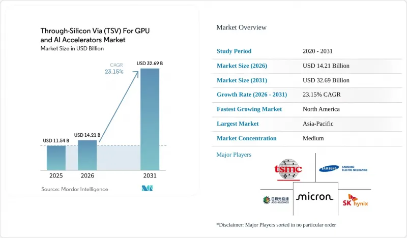
According to Mordor Intelligence, the through-Silicon via for GPU and AI accelerators market size was valued at USD 11.54 billion in 2025 and estimated to grow from USD 14.21 billion in 2026 to reach USD 32.69 billion by 2031, at a CAGR of 23.15% during the forecast period (2026-2031).
This report is Segmented by Architecture (2. 5D TSV Interposer-Based, and 3D TSV Die Stacking), Application (HBM Memory Stacks, GPU Logic-Memory Integration, AI Accelerators and HPC GPUs, and Chiplet-Based GPU Architectures), and Geography (North America, Europe, Asia-Pacific, South America, and Middle East and Africa). The Market Forecasts are Provided in Terms of Value (USD).
Global Through-Silicon Via (TSV) For GPU And AI Accelerators Market Trends and Insights
Mainstream Adoption of HBM3 and Beyond in AI GPUs
HBM3E and HBM4 are lifting TSV density targets above 100,000 vias per package, which redefines packaging cost structures and process windows. SK hynix validated 12-layer HBM4 samples exceeding 2 Tbit-s bandwidth and plans mass production in late 2025. NVIDIA's Rubin GPU, disclosed in 2026, integrates 288 GB of HBM4 and relies on 16-layer stacks that still fit existing server z-height limits because Samsung demonstrated a 12-layer 3D-TSV package that maintains the 720 µm profile of legacy 8-layer HBM2. Memory vendors are now outsourcing base-die logic to leading-edge logic foundries, increasing TSV alignment tolerances and copper-to-copper bonding requirements. These changes are rapidly scaling the Through-Silicon Via market for GPU and AI accelerators as suppliers race to deliver reliable, high-aspect-ratio vias.
Growth of Chiplet-Based GPU Designs Requiring Advanced Interposers
Disaggregating monolithic GPUs into chiplets improves die yield and speeds product refreshes. AMD's MI300A combines 5 nm compute tiles, 6 nm IO tiles, and HBM3 on a single CoWoS-S interposer and delivers over 5 TB-s memory bandwidth. Intel pushed sub-10 µm hybrid-bond pitch with Foveros Direct, enabling vertically stacked voltage regulators and logic layers. The Universal Chiplet Interconnect Express standard, co-led by Samsung, published an open die-to-die PHY in 2024, making interposer access less proprietary. These advances expand demand for large silicon interposers, boosting the Through-Silicon Via market for GPU and AI accelerators.
Yield Challenges in High-Density TSV Fabrication
TSV aspect ratios now exceed 10:1 with diameters below 5 µm, stressing etch, fill, and reveal steps. IEEE research showed that TSV-induced stress shifts transistor thresholds, forcing the use of keep-out zones that erode silicon area. Chipmetrics' inline void detection identified latent failures caused by copper voiding after thermal cycling. Applied Materials released a plasma-wet TSV reveal module that strips dielectric residue without copper damage to raise near-term yields. Until such fixes mature, production output for Through-Silicon Via for GPU and AI accelerators market devices remains gated by defect density.
Other drivers and restraints analyzed in the detailed report include:
- Increasing Capital Investments in 2.5D and 3D Packaging Facilities
- Government Incentives for Domestic Semiconductor Supply Chains
- Thermal Management Limitations in Stacked GPU Modules
For complete list of drivers and restraints, kindly check the Table Of Contents.
Segment Analysis
The 2.5D TSV interposer segment held 68% of the Through-Silicon Via market share for GPU and AI accelerators in 2025, driven by mature design rules and established substrate ecosystems. TSMC's CoWoS-S supports interposers approaching 2,700 mm2, accommodating multiple GPU chiplets and eight or more HBM cubes on one substrate. Samsung's I-CubeE blends silicon bridges with fan-out redistribution layers to lower the cost for large-area interposers. These proven routes ensure high tape-out velocity and predictable yield, sustaining the segment's scale in the Through-Silicon Via market for GPU and AI accelerators during the early forecast years.
3D die-stacking, though only 32% of the 2025 value, is growing at 23.56% CAGR as hybrid copper bonding enables sub-4 µm vertical pitch. Intel's Foveros Direct and Samsung's X-Cube target fine-pitch copper-to-copper joints that trim via parasitics and shorten interlogic paths. TSMC's SoIC promises sub-1 µm pitch, useful for SRAM-on-logic stacks in future GPUs. As equipment yields improve, the 3D route is expected to capture incremental Through-Silicon Via market share for the GPU and AI accelerator market, tied to ultrahigh-bandwidth memory fabrics.
Geography Analysis
Asia-Pacific dominated the Through-Silicon Via for GPU and AI accelerators market in 2025 with a 62% revenue share, driven by TSMC, Samsung, and SK Hynix's cluster fabrication, advanced packaging, and HBM output in Taiwan and South Korea. TSMC's Kumamoto R&D center in Japan co-locates substrate and materials partners, tightening supply cycles for CoWoS roadmap updates. Tokyo Electron scaled 2025 R&D spend to JPY 250.0 billion (USD 1.61 billion) to accelerate the release of bonding equipment and reinforce the regional ecosystem. Export-control headwinds limit China's ability to secure advanced lithography, constraining domestic TSV capacity and limiting its local share of the Through-Silicon Via market for GPU and AI accelerators.
North America's forecast CAGR of 24.15% is driven by hyperscaler demand and government subsidies. TSMC's multi-fab Arizona campus reserves CoWoS lines for U.S. GPU customers, while Amkor's Peoria plant brings an OSAT alternative onshore. Intel's CHIPS-backed Ohio and Arizona expansions promise captive and merchant 3D packaging volumes. The increasing investments in U.S. data-center infrastructure, with AI accelerators emerging as the fastest-growing spend category, are further amplifying domestic demand.
Europe captures a modest but rising share thanks to the EUR 43 billion (approximately USD 46.44 billion) EU Chips Act pool, which finances pilot lines for wafer-level bonding and RDL interposers. STMicroelectronics, GlobalFoundries, and IMEC collaborate on heterogeneous integration test lines, but the absence of a local HBM supply continues to push European GPU designers to Asian memory vendors. South Am, the Middle East End Africa remain marginal, hosting only legacy back-end operations without TSV capacity.
- Taiwan Semiconductor Manufacturing Company Limited (TSMC)
- Samsung Electronics Co., Ltd.
- Micron Technology, Inc.
- SK hynix Inc.
- ASE Technology Holding Co., Ltd.
- Intel Corporation
- Amkor Technology, Inc.
- JCET Group Co., Ltd.
- Powertech Technology Inc.
- Siliconware Precision Industries Co., Ltd.
- United Microelectronics Corporation
- GLOBALFOUNDRIES Inc.
- Broadcom, Inc.
- Cadence Design Systems, Inc.
- Synopsys, Inc.
- Lam Research Corporation
- Applied Materials, Inc.
- Tokyo Electron Limited
- Onto Innovation Inc.
- EVG (EV Group)
Additional Benefits:
- The market estimate (ME) sheet in Excel format
- 3 months of analyst support
TABLE OF CONTENTS
1 INTRODUCTION
- 1.1 Study Assumptions and Market Definition
- 1.2 Scope of the Study
2 RESEARCH METHODOLOGY
3 EXECUTIVE SUMMARY
4 MARKET LANDSCAPE
- 4.1 Market Overview
- 4.2 Market Drivers
- 4.2.1 Mainstream Adoption of HBM3 and Beyond in AI GPUs
- 4.2.2 Growth of Chiplet-Based GPU Designs Requiring Advanced Interposers
- 4.2.3 Increasing Capital Investments in 2.5D/3D Packaging Facilities
- 4.2.4 Government Incentives for Domestic Semiconductor Supply Chains
- 4.2.5 Emerging Hybrid Bonding TSV Techniques for Performance Boost
- 4.2.6 Rising Demand for Energy-Efficient Data Center Accelerators
- 4.3 Market Restraints
- 4.3.1 Yield Challenges in High-Density TSV Fabrication
- 4.3.2 Thermal Management Limitations in Stacked GPU Modules
- 4.3.3 Supply Chain Vulnerabilities to Specialty TSV Equipment
- 4.3.4 Availability of Alternative Advanced Packaging
- 4.4 Impact of Macroeconomic Factors on the Market
- 4.5 Industry Value Chain Analysis
- 4.6 Regulatory Landscape
- 4.7 Technological Outlook
- 4.8 Porter's Five Forces Analysis
- 4.8.1 Bargaining Power of Suppliers
- 4.8.2 Bargaining Power of Buyers
- 4.8.3 Threat of New Entrants
- 4.8.4 Threat of Substitutes
- 4.8.5 Intensity of Competitive Rivalry
5 MARKET SIZE AND GROWTH FORECASTS (VALUE)
- 5.1 By Architecture
- 5.1.1 2.5D TSV (Interposer-based)
- 5.1.2 3D TSV (Die stacking)
- 5.2 By Application
- 5.2.1 HBM Memory Stacks
- 5.2.2 GPU Logic-Memory Integration
- 5.2.3 AI Accelerators / HPC GPUs
- 5.2.4 Chiplet-based GPU Architectures
- 5.3 By Geography
- 5.3.1 North America
- 5.3.1.1 United States
- 5.3.1.2 Canada
- 5.3.1.3 Mexico
- 5.3.2 Europe
- 5.3.2.1 United Kingdom
- 5.3.2.2 Germany
- 5.3.2.3 France
- 5.3.2.4 Rest of Europe
- 5.3.3 Asia-Pacific
- 5.3.3.1 China
- 5.3.3.2 Japan
- 5.3.3.3 India
- 5.3.3.4 South Korea
- 5.3.3.5 Rest of Asia-Pacific
- 5.3.4 South America
- 5.3.5 Middle East and Africa
- 5.3.1 North America
6 COMPETITIVE LANDSCAPE
- 6.1 Market Concentration
- 6.2 Strategic Moves
- 6.3 Market Share Analysis
- 6.4 Company Profiles (includes Global Level Overview, Market Level Overview, Core Segments, Financials as available, Strategic Information, Market Rank/Share, Products and Services, Recent Developments)
- 6.4.1 Taiwan Semiconductor Manufacturing Company Limited (TSMC)
- 6.4.2 Samsung Electronics Co., Ltd.
- 6.4.3 Micron Technology, Inc.
- 6.4.4 SK hynix Inc.
- 6.4.5 ASE Technology Holding Co., Ltd.
- 6.4.6 Intel Corporation
- 6.4.7 Amkor Technology, Inc.
- 6.4.8 JCET Group Co., Ltd.
- 6.4.9 Powertech Technology Inc.
- 6.4.10 Siliconware Precision Industries Co., Ltd.
- 6.4.11 United Microelectronics Corporation
- 6.4.12 GLOBALFOUNDRIES Inc.
- 6.4.13 Broadcom, Inc.
- 6.4.14 Cadence Design Systems, Inc.
- 6.4.15 Synopsys, Inc.
- 6.4.16 Lam Research Corporation
- 6.4.17 Applied Materials, Inc.
- 6.4.18 Tokyo Electron Limited
- 6.4.19 Onto Innovation Inc.
- 6.4.20 EVG (EV Group)
7 MARKET OPPORTUNITIES AND FUTURE OUTLOOK
- 7.1 White-Space and Unmet-Need Assessment

