
PUBLISHER: Mordor Intelligence | PRODUCT CODE: 2062173

PUBLISHER: Mordor Intelligence | PRODUCT CODE: 2062173
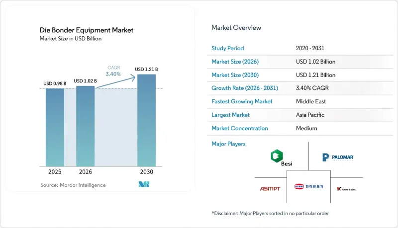
Die Bonder Equipment - Market Share Analysis, Industry Trends & Statistics, Growth Forecasts (2026 - 2031)
According to Mordor Intelligence, the die bonder equipment market size is expected to increase from USD 0.98 billion in 2025 to USD 1.02 billion in 2026 and reach USD 1.21 billion by 2031, growing at a CAGR of 3.40% over 2026-2031.
This report is Segmented by Equipment Type (Fully-Automatic Die Bonders, and More), Bonding Technology (Epoxy/Adhesive Die Attach, and More), Throughput Category (Greater Than 60k UPH, and More), End-Use Industry (Integrated Device Manufacturers, and More), Device Type (Logic and Memory IC, Power and RF, and More), and Geography. The Market Forecasts are Provided in Terms of Value (USD).
Global Die Bonder Equipment Market Trends and Insights
Heterogeneous-Integration and Chiplet Boom
Chiplet partitioning breaks monolithic system-on-chip designs into smaller tiles connected by fine-pitch die-to-die links, slashing reticle cost and improving yield while demanding placement accuracy tighter than 2 µm. Early high-volume shipments of chiplet CPUs validated the economics and triggered a shift from wire bonding toward thermocompression platforms that process one bond instead of dozens of wires, raising tool utilization and justifying higher capital outlays. Universal Chiplet Interconnect Express is standardizing protocols, making advanced packaging accessible to second-tier device makers and expanding the die bonder equipment market. Suppliers are responding with dual-gantry systems, interferometric sensors, and machine-learning alignment engines that cut setup time and improve first-pass yield. The payoff for customers is a mix-and-match design flow that extends Moore's Law economically even as front-end scaling slows.
Advanced 2.5D 3D And Hybrid Bonding Adoption
Hybrid bonding fuses copper pads and dielectric layers at around 200 °C, eliminating microbumps and lifting connection density above 10,000 links mm-2, a prerequisite for next-generation high-bandwidth memory and graphics accelerators. Tool vendors are co-optimizing wafer-to-wafer bonders with planarization steps to keep copper dishing below 5 nm and overlay error under 200 nm. Nanotwinned copper is widening the thermal process window, making organic substrates viable for fine-pitch 3D stacking. Because hybrid-bonding lines cost 50-70% more than flip-chip lines, adoption is initially concentrated at top-tier IDMs and OSATs that can amortize multi-million-dollar tool sets across high-volume programs. Once HBM generation 5 ramps after 2028, a material replacement wave will cascade through memory and logic supply chains, accelerating demand for hybrid-ready die bonders.
Ultra-High-Precision CapEx Burden For Mid-Tier OSATs
A wafer-to-wafer bonder with sub-500 nm overlay costs USD 3-5 million versus USD 1-1.5 million for a mature flip-chip tool, stretching balance sheets at second-tier providers that serve cost-sensitive markets. Ancillary metrology and cleanroom upgrades add another USD 1-2 million, and financing from regional banks can take nine months to approve, delaying expansion plans. Equipment-as-a-service contracts partly offset the burden but come with volume guarantees that smaller players cannot always meet. The result is a widening technology gap between top-tier and mid-tier OSATs, concentrating advanced-packaging revenue and limiting industry-wide adoption speed.
Other drivers and restraints analyzed in the detailed report include:
- Rapid Uptake of Compound-Semiconductor Power Devices
- Data-Center Photonics and Co-Packaged Optics Demand
- Sub-Micron Alignment Yield-Loss Risk
For complete list of drivers and restraints, kindly check the Table Of Contents.
Segment Analysis
Fully automatic systems dominate high-volume logic and memory lines because they deliver sub-0.5 s cycle times and integrate vision, force control, and metrology. The die bonder equipment market size for fully automatic platforms reflects deep penetration among large IDMs and OSATs. Semi-automatic machines serve power and radio-frequency packages that require mixed tooling, while manual and prototype stations stay relevant in R and D. Wafer-to-wafer bonders, growing fastest, eliminate pick-and-place steps and enable connection densities above 10,000 links mm-2, positioning them for 3D chiplet stacks.
Demand for wafer-level machines is rising as foundries scale 3D integration lines capable of more than 1,000 wafers a month. Suppliers bundle vacuum handling, CMP interfaces, and inline inspection to guarantee overlay across 300 mm substrates, differentiating on process control rather than raw speed. Manual bonders remain indispensable for photonics where active alignment with live optical feedback is required. Semi-automatic tools find a niche in automotive modules, balancing flexibility and cost.
Flip-chip, including copper-pillar attach, commands the largest slice thanks to its maturity and compatibility with organic laminates. The die bonder equipment market share for flip-chip is expected to erode slowly as hybrid bonding ramps after 2028. Epoxy attach stays popular in consumer and industrial devices where cost and thermal budget trump density, while eutectic attach secures aerospace and medical applications that mandate hermeticity.
Hybrid bonding's momentum hinges on memory roadmaps that move to direct copper-to-copper links for bandwidth beyond 2 TB s-1. Vendors co-develop bonders and CMP steps to hit <5 nm copper dishing and <200 nm overlay. Thermocompression remains the bridge technology, already displacing solder reflow in fine-pitch flip-chip and radio-frequency modules. Over time, cost parity and density demands will swing share toward hybrid platforms, expanding the die bonder equipment market size for direct Cu-Cu tools.
Geography Analysis
Asia-Pacific anchors more than half of global capacity, underpinned by Taiwan's advanced packaging, China's localization push, and South Korea's memory footprint. Government funding in the United States spurs multiple back-end fabs expected online by 2027, lifting North American equipment shipments. Europe invests in compound-semiconductor packaging in Germany and France to secure supply for electric vehicles and industrial drives. The Middle East emerges as a greenfield investor, channelling sovereign capital into assembly plants slated for first output after 2028.
Tool vendors in Asia-Pacific enjoy proximity advantages, shorter service cycles, and government incentives that subsidize local sourcing. North American purchases skew toward high-precision, high-automation tools compatible with hybrid bonding and wafer-to-wafer stacking. European demand favours silver-sinter and copper-clip compatible platforms for power modules. Middle East orders emphasize turnkey lines bundled with training to expedite ecosystem buildup. South America and Africa remain nascent, limited to academic and prototype installations.
Capacity moves ripple through supply chains: Taiwan's expansion alone requires more than 50 wafer-to-wafer bonders, and U.S. CHIPS Act awards reserve slots at suppliers' months ahead. Chinese entrants undercut pricing on mature flip-chip tools, but advanced equipment still flows mainly from incumbent global brands. Regionalization of semiconductor supply pushes tool vendors to expand local support teams, warehouses, and refurbish centers, raising fixed cost but shortening downtime for customers.
- ASMPT Ltd.
- Kulicke and Soffa Industries Inc.
- BE Semiconductor Industries N.V.
- Hanmi Semiconductor Co., Ltd.
- Palomar Technologies Inc.
- SHINKAWA Ltd.
- Panasonic Holdings Corp. (Factory Solutions)
- SUSS MicroTec SE
- Toray Engineering Co., Ltd.
- TOWA Corporation
- West-Bond Inc.
- MRSI Systems (Mycronic AB)
- Finetech GmbH & Co. KG
- Canon Machinery Inc.
- DIAS Automation (Shenzhen) Co., Ltd.
- F&K Delvotec Bondtechnik GmbH
- Tresky AG
- Hybond Inc.
- Integra Technologies LLC
- EV Group (EVG)
Additional Benefits:
- The market estimate (ME) sheet in Excel format
- 3 months of analyst support
TABLE OF CONTENTS
1 INTRODUCTION
- 1.1 Study Assumptions and Market Definition
- 1.2 Scope of the Study
2 RESEARCH METHODOLOGY
3 EXECUTIVE SUMMARY
4 MARKET LANDSCAPE
- 4.1 Market Overview
- 4.2 Market Drivers
- 4.2.1 Heterogeneous-Integration and Chiplet Boom
- 4.2.2 Advanced 2.5D/3D and Hybrid Bonding Adoption
- 4.2.3 Rapid Uptake of Compound-Semiconductor Power Devices
- 4.2.4 Data-Center Photonics and Co-Packaged Optics Demand
- 4.2.5 Government On-Shoring Subsidies for Back-End Fabs
- 4.2.6 Industry 4.0 Push for Fully-Automatic High-UPH Bonders
- 4.3 Market Restraints
- 4.3.1 Ultra-High-Precision CapEx Burden for Mid-Tier OSATs
- 4.3.2 Sub-Micron Alignment Yield-Loss Risk
- 4.3.3 Precision Component Supply-Chain Bottlenecks
- 4.3.4 Fast Technology Obsolescence Risk in Bonding Tools
- 4.4 Industry Supply-Chain Analysis
- 4.5 Regulatory Landscape
- 4.6 Technological Outlook
- 4.7 Porter's Five Forces Analysis
- 4.7.1 Threat of New Entrants
- 4.7.2 Bargaining Power of Suppliers
- 4.7.3 Bargaining Power of Buyers
- 4.7.4 Threat of Substitutes
- 4.7.5 Intensity of Competitive Rivalry
- 4.8 Impact of Macroeconomic Factors on the Market
5 MARKET SIZE AND GROWTH FORECASTS (VALUE)
- 5.1 By Equipment Type
- 5.1.1 Fully-Automatic Die Bonders
- 5.1.2 Semi-Automatic Die Bonders
- 5.1.3 Manual / Prototype Bonders
- 5.1.4 Wafer-to-Wafer Bonders
- 5.2 By Bonding Technology
- 5.2.1 Epoxy / Adhesive Die Attach
- 5.2.2 Eutectic Die Attach
- 5.2.3 Flip-Chip (C4/Cu-Pillar)
- 5.2.4 Thermocompression and Thermosonic
- 5.2.5 Hybrid and Direct Cu-Cu Bonding
- 5.3 By Throughput Category (Units per Hour)
- 5.3.1 Greater Than 60 k UPH (High-Speed)
- 5.3.2 30-60 k UPH (Mid-Speed)
- 5.3.3 Below 30 k UPH (Low-Speed / High-Precision)
- 5.4 By End-Use Industry
- 5.4.1 Integrated Device Manufacturers (IDMs)
- 5.4.2 Outsourced Semiconductor Assembly and Test (OSATs)
- 5.4.3 Research and Prototyping Labs
- 5.5 By Device Type
- 5.5.1 Logic and Memory IC
- 5.5.2 Power and RF (SiC, GaN)
- 5.5.3 Photonics / Optical Transceivers
- 5.5.4 MEMS and Sensors
- 5.6 By Geography
- 5.6.1 North America
- 5.6.1.1 United States
- 5.6.1.2 Canada
- 5.6.1.3 Mexico
- 5.6.2 South America
- 5.6.2.1 Brazil
- 5.6.2.2 Argentina
- 5.6.2.3 Rest of South America
- 5.6.3 Europe
- 5.6.3.1 Germany
- 5.6.3.2 United Kingdom
- 5.6.3.3 France
- 5.6.3.4 Italy
- 5.6.3.5 Spain
- 5.6.3.6 Rest of Europe
- 5.6.4 Asia-Pacific
- 5.6.4.1 China
- 5.6.4.2 Japan
- 5.6.4.3 South Korea
- 5.6.4.4 India
- 5.6.4.5 Rest of Asia-Pacific
- 5.6.5 Middle East
- 5.6.5.1 Saudi Arabia
- 5.6.5.2 United Arab Emirates
- 5.6.5.3 Rest of Middle East
- 5.6.6 Africa
- 5.6.6.1 South Africa
- 5.6.6.2 Rest of Africa
- 5.6.1 North America
6 COMPETITIVE LANDSCAPE
- 6.1 Market Concentration
- 6.2 Strategic Moves
- 6.3 Market Share Analysis
- 6.4 Company Profiles (includes Global Level Overview, Market Level Overview, Core Segments, Financials as available, Strategic Information, Market Rank/Share, Products and Services, Recent Developments)
- 6.4.1 ASMPT Ltd.
- 6.4.2 Kulicke and Soffa Industries Inc.
- 6.4.3 BE Semiconductor Industries N.V.
- 6.4.4 Hanmi Semiconductor Co., Ltd.
- 6.4.5 Palomar Technologies Inc.
- 6.4.6 SHINKAWA Ltd.
- 6.4.7 Panasonic Holdings Corp. (Factory Solutions)
- 6.4.8 SUSS MicroTec SE
- 6.4.9 Toray Engineering Co., Ltd.
- 6.4.10 TOWA Corporation
- 6.4.11 West-Bond Inc.
- 6.4.12 MRSI Systems (Mycronic AB)
- 6.4.13 Finetech GmbH & Co. KG
- 6.4.14 Canon Machinery Inc.
- 6.4.15 DIAS Automation (Shenzhen) Co., Ltd.
- 6.4.16 F&K Delvotec Bondtechnik GmbH
- 6.4.17 Tresky AG
- 6.4.18 Hybond Inc.
- 6.4.19 Integra Technologies LLC
- 6.4.20 EV Group (EVG)
7 MARKET OPPORTUNITIES AND FUTURE OUTLOOK
- 7.1 White-Space and Unmet-Need Assessment

