
PUBLISHER: Mordor Intelligence | PRODUCT CODE: 2063399

PUBLISHER: Mordor Intelligence | PRODUCT CODE: 2063399
Silicon Wafer For Logic Devices - Market Share Analysis, Industry Trends & Statistics, Growth Forecasts (2026 - 2031)
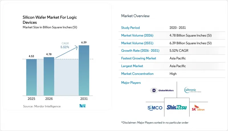
According to Mordor Intelligence, the silicon wafer market for Logic Devices market size is projected to be 4.53 billion square inches in 2025, 4.78 billion square inches in 2026, and reach 6.39 billion square inches by 2031, growing at a CAGR of 5.52% from 2026 to 2031.
This report is Segmented by Wafer Diameter (≤150mm, 200mm, and 300mm), Wafer Type (Prime Polished, Epitaxial, Silicon-On-Insulator (SOI), and Specialty Silicon (High-Resistivity, Power, and More)), End-User Application (Consumer Electronics, Industrial, Telecommunications, Automotive, and More), and Geography. The Market Forecasts are Provided in Terms of Shipment Area (Billion Square Inches).
Insights and Trends of Silicon Wafer Market For Logic Devices
Growing Demand for AI and High-Performance Computing Chips
Hyperscalers are shipping custom accelerators in ever-larger training clusters, and each cluster can consume more than 10,000 substrates per quarter as GPU, networking, and chiplet base dies all originate on 300 mm silicon. Chiplet partitioning increases overall wafer starts because interposer and base dies join the demand profile, even as transistor density rises per chip. Leading-edge foundry nodes such as N3, N2, and 18A report double-digit revenue shares, signaling sustained appetite for ultra-flat, low-defect substrates that ensure high yields. Edge-inference deployments widen the diameter mix by drawing mature 7 nm and 5 nm lines into automotive and industrial environments, pushing total substrate volume higher. This driver therefore reinforces both advanced and mature-node demand streams for the Silicon Wafer Market for Logic Devices market.
Transition Toward 3 nm and Below Nodes Using 300 mm Wafers
The cost of extreme ultraviolet lithography tools in excess of USD 200 million per unit necessitates 300 mm wafer platforms, concentrating capacity and capital on one diameter. Gate-all-around nanosheet transistors and backside power delivery networks require epitaxial source-drain regions on substrates with total thickness variation below 0.15 micrometers, tightening flatness requirements well beyond the SEMI M1 baseline. Samsung, Intel, and foundry peers now specify sub-angstrom surface roughness, spurring wafer-maker investment in chemical-mechanical polishing and laser metrology. As nodes shrink, each exposure step tolerates fewer particles, so 300 mm crystal defect density must trend downward, locking in higher value per wafer and sustaining the Silicon Wafer Market for Logic Devices market.
High Capital Expenditure for 300 mm Wafer Capacity
A greenfield 300 mm wafer plant requires USD 3 billion-USD 5 billion upfront, and equipment depreciation spans 10-15 years, increasing financial risk for prospective entrants. Rising interest rates in 2024-2025 lifted weighted-average cost of capital by up to 200 basis points, delaying expansion at second-tier suppliers. GlobalWafers' USD 5 billion Texas fab, announced in 2025 yet slated for 2028 ramp, underlines the long payback cycles that constrain supply elasticity. High capex narrows the field to five dominant vendors, moderating competitive pricing in the Silicon Wafer Market for Logic Devices market.
Other drivers and restraints analyzed in the detailed report include:
- Rising Investment in Front-End Fabs Under Government Incentives
- Expansion of 5G and IoT Device Production Volumes
- Supply Chain Disruptions in Polysilicon and Specialty Gases
For complete list of drivers and restraints, kindly check the Table Of Contents.
Segment Analysis
The 300 mm class held 86.87% of 2025 shipments and is advancing at a 6.04% CAGR, underscoring its structural cost advantage in the Silicon Wafer Market for Logic Devices market. A single 300 mm wafer yields nearly 2.4 times the die count of a 200 mm substrate of equal design, lowering cost per transistor by up to 40%. All leading-edge capacity additions through 2031 are earmarked for this diameter, channeling supplier capex and reinforcing a virtuous cycle of scale.
Foundries still operate 200 mm lines for power-management, analog, and MEMS circuits, but equipment obsolescence and tool scarcity are pushing even these workloads onto 300 mm. Sub-150 mm wafers now account for less than 5% of logic shipments, making them a legacy niche. As Siltronic and SK Siltron shutter 150 mm production by 2027, slow-moving aerospace and military programs will bear re-qualification costs, yet mainstream economics leave suppliers few alternatives, solidifying 300 mm leadership within the Silicon Wafer Market for Logic Devices market.
Geography Analysis
Asia-Pacific retained 78.68% shipment share in 2025 and is expanding at 6.17% CAGR through 2031 as Taiwan, South Korea, and mainland China extend advanced-node capacity. TSMC alone consumed more than 1 million 300 mm wafers monthly across 13 fabs, and two additional Kaohsiung plants come online by 2028. Samsung's Hwaseong campus entered 2 nm production in late 2025, while SK Siltron increased Gumi pulls to serve domestic customers. China's drive for self-reliance maintains demand despite export controls, aided by local suppliers Ferrotec and Shanghai Simgui.
North America is re-emerging, powered by USD 52.7 billion in CHIPS Act grants. Intel's Arizona and Ohio projects plus TSMC's Phoenix complex will together draw roughly 400,000 wafers per month by 2027. GlobalWafers' Texas plant, slated for 2028, marks the first large-scale domestic substrate output in two decades, shrinking logistics lead times. Sustainability rules tighten water-use metrics; TSMC Arizona already recycles 65% of process water, a benchmark regulators look to codify.
Europe accounted for under 10% of 2025 shipments but is accelerating as the EUR 43 billion (USD 48.6 billion) EU Chips Act sponsors Intel's Magdeburg dual-fab, TSMC's Dresden joint venture with Bosch, and STMicroelectronics, GlobalFoundries FD-SOI expansion in Crolles. Long-term take-or-pay wafer contracts underpin these ventures, lifting regional demand and adding diversity to the Silicon Wafer Market for Logic Devices market. South America and the Middle East and Africa remain peripheral, though sovereign funds in Saudi Arabia considered partnership in 2025 to seed a regional hub, a move watched closely by substrate vendors evaluating long-range diversification.
- Shin-Etsu Chemical Co., Ltd.
- SUMCO Corporation
- GlobalWafers Co., Ltd.
- Siltronic AG
- SK Siltron Co., Ltd.
- Wafer Works Corporation
- Okmetic Oyj
- Soitec S.A.
- S.E.H. Europe GmbH
- Ferrotec Holdings Corporation
- Poshing Technology Co., Ltd.
- LG Siltron Inc.
- Advanced Silicon S.A.
- Topsil Semiconductor Materials A/S
- Sumco Phoenix Corporation
- Hyperion Materials & Technologies
- MTI Corporation
Additional Benefits:
- The market estimate (ME) sheet in Excel format
- 3 months of analyst support
TABLE OF CONTENTS
1 INTRODUCTION
- 1.1 Study Assumptions and Market Definition
- 1.2 Scope of the Study
2 RESEARCH METHODOLOGY
3 EXECUTIVE SUMMARY
4 MARKET LANDSCAPE
- 4.1 Market Overview
- 4.2 Market Drivers
- 4.2.1 Growing Demand for AI and High-Performance Computing Chips
- 4.2.2 Transition Toward 3 nm and Below Nodes Using 300 mm Wafers
- 4.2.3 Rising Investment in Front-End Fabs Under Government Incentives
- 4.2.4 Expansion of 5G and IoT Device Production Volumes
- 4.2.5 Backside Power Delivery Architectures Requiring Ultra-Flat Wafers
- 4.2.6 Silicon Photonics Co-Integration in Logic Devices
- 4.3 Market Restraints
- 4.3.1 High Capital Expenditure for 300 mm Wafer Capacity
- 4.3.2 Supply Chain Disruptions in Polysilicon and Specialty Gases
- 4.3.3 Limited Availability of Ultra-High-Purity Float-Zone Silicon
- 4.3.4 Stricter Water-Use Regulations in Major Fab Locations
- 4.4 Industry Value Chain Analysis
- 4.5 Regulatory Landscape
- 4.6 Technological Outlook
- 4.7 Porter's Five Forces Analysis
- 4.7.1 Bargaining Power of Suppliers
- 4.7.2 Bargaining Power of Buyers
- 4.7.3 Threat of New Entrants
- 4.7.4 Threat of Substitutes
- 4.7.5 Competitive Rivalry
- 4.8 Impact of Macroeconomic Factors on the Market
5 MARKET SIZE AND GROWTH FORECASTS (SHIPMENT IN AREA)
- 5.1 By Wafer Diameter
- 5.1.1 <=150 mm
- 5.1.2 200 mm
- 5.1.3 300 mm
- 5.2 By Wafer Type
- 5.2.1 Prime Polished
- 5.2.2 Epitaxial
- 5.2.3 Silicon-on-Insulator (SOI)
- 5.2.4 Specialty Silicon (High-Resistivity, Power, Sensor-Grade)
- 5.3 By End-user Application
- 5.3.1 Consumer Electronics
- 5.3.1.1 Mobile and Smartphones
- 5.3.1.2 PCs and Servers
- 5.3.2 Industrial
- 5.3.3 Telecommunications
- 5.3.4 Automotive
- 5.3.5 Other End-user Applications
- 5.3.1 Consumer Electronics
- 5.4 By Geography
- 5.4.1 North America
- 5.4.1.1 United States
- 5.4.1.2 Canada
- 5.4.1.3 Mexico
- 5.4.2 Europe
- 5.4.2.1 Germany
- 5.4.2.2 United Kingdom
- 5.4.2.3 France
- 5.4.2.4 Rest of Europe
- 5.4.3 Asia-Pacific
- 5.4.3.1 China
- 5.4.3.2 Japan
- 5.4.3.3 India
- 5.4.3.4 South Korea
- 5.4.3.5 Taiwan
- 5.4.3.6 Rest of Asia-Pacific
- 5.4.4 South America
- 5.4.5 Middle East and Africa
- 5.4.1 North America
6 COMPETITIVE LANDSCAPE
- 6.1 Market Concentration
- 6.2 Strategic Moves
- 6.3 Market Share Analysis
- 6.4 Company Profiles (includes Global Level Overview, Market Level Overview, Core Segments, Financials as available, Strategic Information, Market Rank/Share, Products and Services, Recent Developments)
- 6.4.1 Shin-Etsu Chemical Co., Ltd.
- 6.4.2 SUMCO Corporation
- 6.4.3 GlobalWafers Co., Ltd.
- 6.4.4 Siltronic AG
- 6.4.5 SK Siltron Co., Ltd.
- 6.4.6 Wafer Works Corporation
- 6.4.7 Okmetic Oyj
- 6.4.8 Soitec S.A.
- 6.4.9 S.E.H. Europe GmbH
- 6.4.10 Ferrotec Holdings Corporation
- 6.4.11 Poshing Technology Co., Ltd.
- 6.4.12 LG Siltron Inc.
- 6.4.13 Advanced Silicon S.A.
- 6.4.14 Topsil Semiconductor Materials A/S
- 6.4.15 Sumco Phoenix Corporation
- 6.4.16 Hyperion Materials & Technologies
- 6.4.17 MTI Corporation
7 MARKET OPPORTUNITIES AND FUTURE OUTLOOK
- 7.1 White-Space and Unmet-Need Assessment

