
PUBLISHER: Mordor Intelligence | PRODUCT CODE: 2063400

PUBLISHER: Mordor Intelligence | PRODUCT CODE: 2063400
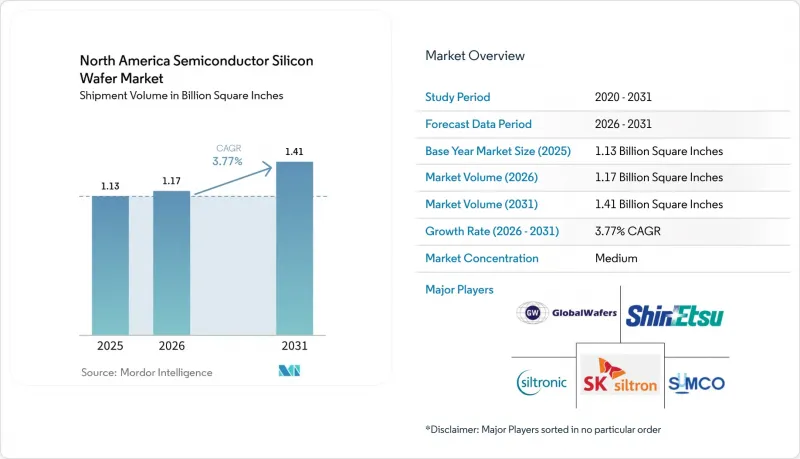
North America Semiconductor Silicon Wafer - Market Share Analysis, Industry Trends & Statistics, Growth Forecasts (2026 - 2031)
According to Mordor Intelligence, the north america semiconductor silicon wafer market size in terms of shipment volume is expected to grow from 1.13 Billion Square Inches in 2025 to 1.17 Billion Square Inches in 2026 and is forecast to reach 1.41 Billion Square Inches by 2031 at a 3.77% CAGR over 2026-2031.
This report is Segmented by Wafer Diameter (Up To 150mm, 200mm, and 300mm), Semiconductor Device Type (Logic, Memory, Analog, Discrete, and More), Wafer Type (Prime Polished, Epitaxial, SOI, and Specialty Silicon), End-User (Consumer Electronics, Industrial, Telecommunications, and More), and Country. The Market Forecasts are Provided in Terms of Volume (Square Inches).
North America Semiconductor Silicon Wafer Market Trends and Insights
Capacity Expansions by Leading Foundries
Massive multiyear investments from TSMC, Intel, and Texas Instruments continue to upgrade the North America semiconductor silicon wafer market. The Arizona gigafab cluster already matches Taiwan yield levels, Intel's Fab 52 has entered high-volume production on 18A, and Texas Instruments has automated its Sherman complex with humanoid robots. Concentrated orders allow substrate suppliers to amortize qualification costs and lock in advance payments, ensuring predictable throughput and quicker node ramps.
Surge in U.S. CHIPS Act Incentives
Direct grants, low-cost loans, and a 25% tax credit lower capital hurdles for every tier of the value chain, from polysilicon to finished wafers. Milestone-based disbursements prevent speculative overbuilding, while clawback clauses protect taxpayers. Wafer makers leverage these subsidies to co-locate with fabs, shortening logistics cycles and enhancing supply resilience for the North America semiconductor silicon wafer market.
Cyclical Memory Downturns
A persistent inventory overhang in commodity DRAM and NAND used up cleanroom space without proportional wafer pull-through in 2025. Price erosion outside long-term contracts cut margins for wafer suppliers, exposing the North America semiconductor silicon wafer market to sharp quarterly swings. Although high-bandwidth memory for AI helps, it cannot fully neutralize volume softness until inventories normalize.
Other drivers and restraints analyzed in the detailed report include:
- Transition Toward 300 mm Wafers in Logic Nodes
- Rising Demand for Si Power Devices in EVs
- Supply Chain Geographic Concentration Risk
For complete list of drivers and restraints, kindly check the Table Of Contents.
Segment Analysis
The 300 mm slice of the North America semiconductor silicon wafer market stands at 70.62% volume and gains from leading-edge AI and 3 nm logic ramps, and expanding at a 4.95% CAGR through 2031. Large-die GPUs, high-density DRAM, and highly automated analog lines benefit from a larger surface, spreading lithography cost over more die and lifting gross margins. The North America semiconductor silicon wafer market size attached to 300 mm fabs therefore rises faster than the overall curve, reinforcing demand visibility for suppliers.
200 mm wafers remain crucial for automotive, power, and mature analog, particularly as EV content skyrockets. Capacity additions in onsemi and Infineon lines keep legacy fabs busy, preventing sudden obsolescence. Suppliers juggling both diameters offset demand cliffs and deepen relationships across device generations, which strengthens the North America semiconductor silicon wafer market over the long term.
Logic devices held 33.09% of the 2025 volume and are advancing at a 5.25% CAGR to 2031, as AI inference shifts to smartphones, PCs, and edge servers. RibbonFET and backside power delivery sharpen transistor efficiency, but they also raise crystal quality demands. Wafer makers shipping to these nodes capture price premiums, lifting the North America semiconductor silicon wafer market share tied to logic.
Memory's cyclicality tempers its net contribution despite U.S. DRAM megafab announcements. High-bandwidth memory stacks use more silicon per package, yet soft PC and handset demand restrains overall wafer lifts. Analog and discrete devices post steady, mid-single-digit volume growth, balancing the portfolio for substrates suppliers targeting industrial and telecom customers.
List of Companies Covered in this Report:
- Shin-Etsu Chemical Co., Ltd.
- SUMCO Corporation
- GlobalWafers Co., Ltd.
- Siltronic AG
- SK Siltron Co., Ltd.
- Wafer Works Corporation
- Okmetic Oy
- Soitec SA
- Sil'Tronix Silicon Technologies
- SunEdison Semiconductor Ltd.
- Zhonghuan Semiconductor Co., Ltd.
- Simgui Technology Co., Ltd.
- Topsil Semiconductor Materials A/S
- Virginia Semiconductor Inc.
- Addison Engineering, Inc.
- University Wafer, Inc.
- Valley Design Corp.
- Pure Wafer PLC
- NOVA Electronic Materials, LLC
- Wafer World Inc.
Additional Benefits:
- The market estimate (ME) sheet in Excel format
- 3 months of analyst support
TABLE OF CONTENTS
1 INTRODUCTION
- 1.1 Study Assumptions and Market Definition
- 1.2 Scope of the Study
2 RESEARCH METHODOLOGY
3 EXECUTIVE SUMMARY
4 MARKET LANDSCAPE
- 4.1 Market Overview
- 4.2 Market Drivers
- 4.2.1 Soaring Demand for 300 mm Wafers from AI Accelerator Fabs
- 4.2.2 CHIPS Act Incentives Catalyzing Local Wafer Production
- 4.2.3 Rapid Adoption of Electric Vehicles Boosting Power Device Wafers
- 4.2.4 Transition Toward Specialty Silicon for SiC and GaN Devices
- 4.2.5 Miniaturization Roadmap to 2 nm Nodes Requiring Ultra-Flat Prime Wafers
- 4.2.6 Reshoring Initiatives Reducing Supply-Chain Risk
- 4.3 Market Restraints
- 4.3.1 Volatile Polysilicon Prices Squeezing Supplier Margins
- 4.3.2 Lengthy Environmental Permitting Delays for New Fabs
- 4.3.3 Competition from Asian 300 mm Megafabs Limiting Utilization
- 4.3.4 Smartphone Market Slowdown Dampening Legacy Wafer Demand
- 4.4 Industry Value Chain Analysis
- 4.5 Regulatory Landscape
- 4.6 Impact of Macroeconomic Factors on the Market
- 4.7 Technological Outlook
- 4.8 Porter's Five Forces Analysis
- 4.8.1 Bargaining Power of Suppliers
- 4.8.2 Bargaining Power of Buyers
- 4.8.3 Threat of New Entrants
- 4.8.4 Threat of Substitutes
- 4.8.5 Intensity of Competitive Rivalry
5 MARKET SIZE AND GROWTH FORECASTS (VOLUME)
- 5.1 By Wafer Diameter
- 5.1.1 Up to 150 mm
- 5.1.2 200 mm
- 5.1.3 300 mm
- 5.2 By Semiconductor Device Type
- 5.2.1 Logic
- 5.2.2 Memory
- 5.2.3 Analog
- 5.2.4 Discrete
- 5.2.5 Other Semiconductor Device Types (Optoelectronics, Sensors, Micro)
- 5.3 By Wafer Type
- 5.3.1 Prime Polished
- 5.3.2 Epitaxial
- 5.3.3 Silicon-on-Insulator (SOI)
- 5.3.4 Specialty Silicon (High-Resistivity, Power, Sensor-Grade)
- 5.4 By End-user
- 5.4.1 Consumer Electronics
- 5.4.1.1 Mobile and Smartphones
- 5.4.1.2 PCs and Servers
- 5.4.2 Industrial
- 5.4.3 Telecommunications
- 5.4.4 Automotive
- 5.4.5 Other End-user Applications
- 5.4.1 Consumer Electronics
- 5.5 By Country
- 5.5.1 United States
- 5.5.2 Canada
- 5.5.3 Mexico
6 COMPETITIVE LANDSCAPE
- 6.1 Market Concentration
- 6.2 Strategic Moves
- 6.3 Market Share Analysis
- 6.4 Company Profiles (includes Global Level Overview, Market Level Overview, Core Segments, Financials as available, Strategic Information, Market Rank/Share, Products and Services, Recent Developments)
- 6.4.1 Shin-Etsu Chemical Co., Ltd.
- 6.4.2 SUMCO Corporation
- 6.4.3 GlobalWafers Co., Ltd.
- 6.4.4 Siltronic AG
- 6.4.5 SK Siltron Co., Ltd.
- 6.4.6 Wafer Works Corporation
- 6.4.7 Okmetic Oy
- 6.4.8 Soitec SA
- 6.4.9 Sil'Tronix Silicon Technologies
- 6.4.10 SunEdison Semiconductor Ltd.
- 6.4.11 Zhonghuan Semiconductor Co., Ltd.
- 6.4.12 Simgui Technology Co., Ltd.
- 6.4.13 Topsil Semiconductor Materials A/S
- 6.4.14 Virginia Semiconductor Inc.
- 6.4.15 Addison Engineering, Inc.
- 6.4.16 University Wafer, Inc.
- 6.4.17 Valley Design Corp.
- 6.4.18 Pure Wafer PLC
- 6.4.19 NOVA Electronic Materials, LLC
- 6.4.20 Wafer World Inc.
7 MARKET OPPORTUNITIES AND FUTURE OUTLOOK
- 7.1 White-Space and Unmet-Need Assessment

