
PUBLISHER: Mordor Intelligence | PRODUCT CODE: 2063401

PUBLISHER: Mordor Intelligence | PRODUCT CODE: 2063401
United States Semiconductor Silicon Wafer - Market Share Analysis, Industry Trends & Statistics, Growth Forecasts (2026 - 2031)
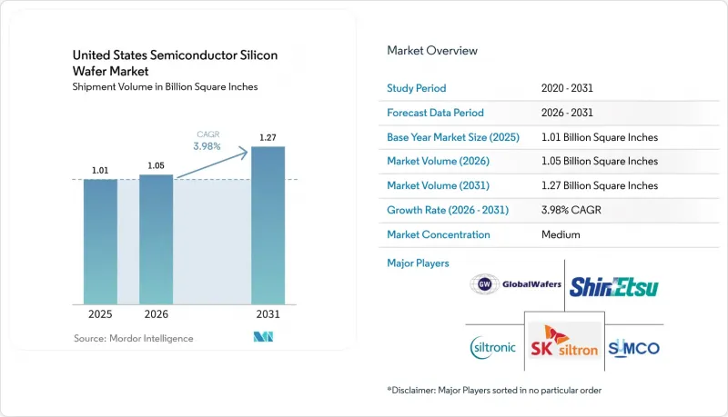
According to Mordor Intelligence, the united states semiconductor silicon wafer market size in terms of shipment volume is projected to be 1.01 Billion Square Inches in 2025, 1.05 Billion Square Inches in 2026, and reach 1.27 Billion Square Inches by 2031, growing at a CAGR of 3.98% from 2026 to 2031.
This report is Segmented by Wafer Diameter (Up To 150mm, 200mm, 300mm), Semiconductor Device Type (Logic, Memory, Analog, Discrete, Other), Wafer Type (Prime Polished, Epitaxial, SOI, Specialty Silicon), and End-User (Consumer Electronics With Mobile and PCs Subsegments, Industrial, Telecommunications, and More). The Market Forecasts are Provided in Terms of Volume (Square Inches).
United States Semiconductor Silicon Wafer Market Trends and Insights
Capacity Expansions by Leading Foundries
Unprecedented capital spending by three global leaders is reshaping the United States semiconductor silicon wafer market. TSMC is installing six mega-fabs and two advanced packaging lines in Arizona, Intel is adding new 18A lines across four states, and Samsung is scaling a two-nanometer logic campus in Texas. Each site will consume millions of 300 millimeter wafers every year once fully qualified. Domestic substrate makers are racing to match that pull, but new crystal-growth and slicing workshops will not reach steady output until 2027, which leaves a two-year window in which foundries remain tied to imports.
Surge in U.S. CHIPS Act Incentives
The CHIPS and Science Act lowers the hurdle rate for new plants and has already redirected investments that might have gone to Asia. Matching grants cut the effective cost of a United States wafer line by as much as a fifth and include hard guardrails that block advanced-node expansion in China for a decade. Those terms keep incremental demand local, yet raw polysilicon still arrives from Germany or Japan, meaning supply security is only partially solved.
Cyclical Memory Downturns
DRAM and NAND suppliers cut orders sharply in early 2025 as smartphone sales softened and cloud firms digested inventory. Memory wafers represent nearly one-quarter of the United States semiconductor silicon wafer market, so a single price correction quickly deflates substrate revenue. High-bandwidth memory stays healthy for artificial intelligence servers, but that niche is too small to stabilize overall demand.
Other drivers and restraints analyzed in the detailed report include:
- Transition Toward 300 mm Wafers in Logic Nodes
- Rising Demand for Si Power Devices in EVs
- Supply Chain Geographic Concentration Risk
For complete list of drivers and restraints, kindly check the Table Of Contents.
Segment Analysis
The 300 millimeter slice of the United States semiconductor silicon wafer market size reached 70.62% of volume in 2025 and is forecast to rise at a 4.95% CAGR to 2031. TSMC's and Intel's new Arizona and Ohio fabs alone will add more than 30 million square inches of demand once fully loaded. High die counts per wafer improve cost efficiency, yet only three global suppliers hold a meaningful share of 300 millimeter crystal capacity.
By contrast, 200 millimeter substrates underpin analog, MEMS, and automotive power electronics. That format expanded 14% between 2023 and 2026, but U.S. capacity equals only 14% of global supply. Automakers face a possible shortfall in 2026-2027, when inverter chips will compete with industrial controls for the same wafers. Sub-150 millimeter formats persist in defense and legacy lines but advance just 1.8% a year, reinforcing a three-speed supply picture in which wafer makers must focus investment where volume and margin justify.
Logic captured 33.09% of United States semiconductor silicon wafer market share in 2025 and is tracking a 5.25% CAGR through 2031, propelled by artificial intelligence accelerators that need leading-edge nodes and epitaxial layers. TSMC disclosed that three-nanometer revenue overtook smartphones in late 2025, confirming the momentum behind high-performance computing.
Memory volumes, however, dipped in early 2025 as DRAM and NAND prices softened. Although HBM devices for training clusters stay profitable, they occupy less than 5% of memory wafer volume. Analog and discrete components show steady 3-4% growth in 200 millimeter fabs, while sensors and MEMS stand near the same pace, helped by automotive radar and smart speakers.
List of Companies Covered in this Report:
- Shin-Etsu Chemical Co., Ltd.
- SUMCO Corporation
- GlobalWafers Co., Ltd.
- Siltronic AG
- SK siltron Co., Ltd.
- Okmetic Oy
- Wafer Works Corp.
- Siltronic Silicon Wafer Pte Ltd
- Soitec S.A.
- WaferPro
- Tianjin Zhonghuan Semiconductor Co., Ltd.
- Ultrasil Corporation
- Poshing Technology Co., Ltd.
- Advanced Silicon Technologies
- 300mm Wafer Fab LLC
- Virginia Semiconductor, Inc.
- Rogue Valley Microdevices, Inc.
- SKC Solmics Co., Ltd.
- Qromis, Inc.
- Addison Engineering, Inc.
Additional Benefits:
- The market estimate (ME) sheet in Excel format
- 3 months of analyst support
TABLE OF CONTENTS
1 INTRODUCTION
- 1.1 Study Assumptions and Market Definition
- 1.2 Scope of the Study
2 RESEARCH METHODOLOGY
3 EXECUTIVE SUMMARY
4 MARKET LANDSCAPE
- 4.1 Market Overview
- 4.2 Market Drivers
- 4.2.1 Mainstream, Capacity Expansions by Leading Foundries
- 4.2.2 Mainstream, Surge in U.S. CHIPS Act Incentives
- 4.2.3 Mainstream, Transition Toward 300 mm Wafers in Logic Nodes
- 4.2.4 Mainstream, Rising Demand for Si Power Devices in EVs
- 4.2.5 Under-the-Radar, AI-Optimised SOI Wafer Demand
- 4.2.6 Under-the-Radar, Defense-Grade Radiation-Hard Silicon
- 4.3 Market Restraints
- 4.3.1 Mainstream, Cyclical Memory Downturns
- 4.3.2 Mainstream, Supply Chain Geographic Concentration Risk
- 4.3.3 Under-the-Radar, Crystalline Defect Limits at 3 nm and Below
- 4.3.4 Under-the-Radar, Growing Competition from SiC & GaN Substrates
- 4.4 Industry Value Chain Analysis
- 4.5 Regulatory Landscape
- 4.6 Technology Analysis
- 4.7 Impact of Macroeconomic Factors
- 4.8 Porter's Five Forces Analysis
- 4.8.1 Bargaining Power of Suppliers
- 4.8.2 Bargaining Power of Buyers
- 4.8.3 Threat of New Entrants
- 4.8.4 Threat of Substitutes
- 4.8.5 Intensity of Competitive Rivalry
5 MARKET SIZE AND GROWTH FORECASTS (VOLUME)
- 5.1 By Wafer Diameter
- 5.1.1 Up to 150 mm
- 5.1.2 200 mm
- 5.1.3 300 mm
- 5.2 By Semiconductor Device Type
- 5.2.1 Logic
- 5.2.2 Memory
- 5.2.3 Analog
- 5.2.4 Discrete
- 5.2.5 Other Semiconductor Device Types (Optoelectronics, Sensors, Micro)
- 5.3 By Wafer Type
- 5.3.1 Prime Polished
- 5.3.2 Epitaxial
- 5.3.3 Silicon-on-Insulator (SOI)
- 5.3.4 Specialty Silicon (High-Resistivity, Power, Sensor-Grade)
- 5.4 By End-user
- 5.4.1 Consumer Electronics
- 5.4.1.1 Mobile and Smartphones
- 5.4.1.2 PCs and Servers
- 5.4.2 Industrial
- 5.4.3 Telecommunications
- 5.4.4 Automotive
- 5.4.5 Other End-user
- 5.4.1 Consumer Electronics
6 COMPETITIVE LANDSCAPE
- 6.1 Market Concentration
- 6.2 Strategic Moves
- 6.3 Market Share Analysis
- 6.4 Company Profiles (includes Global Level Overview, Market Level Overview, Core Segments, Financials as available, Strategic Information, Market Rank/Share, Products and Services, Recent Developments)
- 6.4.1 Shin-Etsu Chemical Co., Ltd.
- 6.4.2 SUMCO Corporation
- 6.4.3 GlobalWafers Co., Ltd.
- 6.4.4 Siltronic AG
- 6.4.5 SK siltron Co., Ltd.
- 6.4.6 Okmetic Oy
- 6.4.7 Wafer Works Corp.
- 6.4.8 Siltronic Silicon Wafer Pte Ltd
- 6.4.9 Soitec S.A.
- 6.4.10 WaferPro
- 6.4.11 Tianjin Zhonghuan Semiconductor Co., Ltd.
- 6.4.12 Ultrasil Corporation
- 6.4.13 Poshing Technology Co., Ltd.
- 6.4.14 Advanced Silicon Technologies
- 6.4.15 300mm Wafer Fab LLC
- 6.4.16 Virginia Semiconductor, Inc.
- 6.4.17 Rogue Valley Microdevices, Inc.
- 6.4.18 SKC Solmics Co., Ltd.
- 6.4.19 Qromis, Inc.
- 6.4.20 Addison Engineering, Inc.
7 MARKET OPPORTUNITIES AND FUTURE OUTLOOK
- 7.1 White-space and Unmet-Need Assessment

