
PUBLISHER: Mordor Intelligence | PRODUCT CODE: 2066588

PUBLISHER: Mordor Intelligence | PRODUCT CODE: 2066588
High Bandwidth Memory - Market Share Analysis, Industry Trends & Statistics, Growth Forecasts (2026 - 2031)
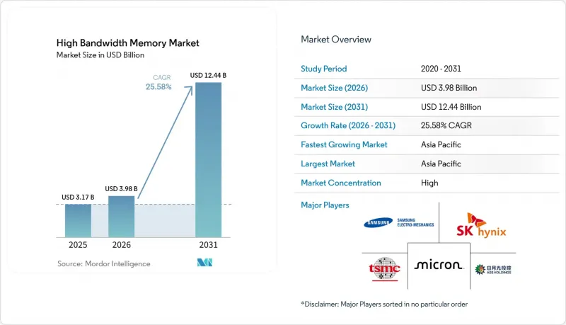
According to Mordor Intelligence, the high bandwidth memory market size is expected to increase from USD 3.17 billion in 2025 to USD 3.98 billion in 2026 and reach USD 12.44 billion by 2031, growing at a CAGR of 25.58% over 2026-2031.
This report is Segmented by Application (Servers, Networking, High-Performance Computing, Consumer Electronics, and Automotive and Transportation), Technology (HBM2, HBM2E, HBM3, HBM3E, and HBM4), Memory Capacity Per Stack (4 GB, 8 GB, 16 GB, 24 GB, and More), Processor Interface (GPU, CPU, AI Accelerator/ASIC, FPGA, and Other Interfaces), and Geography. Market Forecasts are Provided in Terms of Value (USD).
Global High Bandwidth Memory Market Trends and Insights
AI-Server Proliferation and GPU Attach Rates
Enterprises are pivoting toward GPU-dense servers that demand four to eight HBM stacks per node to keep pace with transformer models exceeding one trillion parameters. Dell Technologies reported AI-optimized server revenue up 80% year over year in fiscal 2025, illustrating how traditional OEMs are profiting from this pivot. Non-traditional buyers such as Bitcoin miner-turned-AI provider IREN have ordered 20,000 Nvidia H200 GPUs, each with 141 GB of HBM3E, confirming that bandwidth needs spill across verticals. As model sizes grow, the memory-to-compute ratio continues to climb, locking in multiyear visibility for HBM suppliers. The generational jump from HBM2E to HBM3E raised per-stack bandwidth by 50%, yet developers are already specifying HBM4 for 2027 hardware, compressing product lifecycles and forcing overlapping R&D. Consequently, DRAM makers are capturing a larger share of system bill-of-materials than GPU vendors ever anticipated.
Data-Center Shift to DDR5 and 2.5-D Packaging
Migration from DDR4 to DDR5 has familiarized substrate manufacturers and assembly houses with multi-gigahertz signaling, lowering perceived risk around HBM qualification. By late 2025, DDR5 modules represented over half of server DRAM shipments, and the learning curve in thermal design for 6.4 GT/s interfaces directly benefits HBM packaging. TSMC's Chip-on-Wafer-on-Substrate process routes thousands of micro-bumps between logic and memory dies, a technology that evolved from earlier 2.5-D field-programmable gate arrays. As manufacturing maturity rises, HBM cost premiums have narrowed from 10X to roughly 4X versus commodity DRAM, widening adoption beyond hyperscale AI into high-performance computing and premium graphics cards. Standards bodies have codified interoperability, preventing vendor lock-in and accelerating the diffusion of High Bandwidth Memory across multiple compute domains.
Limited CoWoS/SoIC Advanced-Packaging Capacity
TSMC's CoWoS and SoIC lines reached roughly 120,000 wafers per month by late 2025, but Nvidia alone reserved more than half of that volume for 2026. Short-run alternatives at ASE, Amkor, and JCET offer fan-out or silicon-bridge options, yet these processes lag in yield and customer qualifications, forcing second-tier chip designers to accept longer validation cycles or reduced performance. Although TSMC earmarked part of its USD 44-50 billion in fiscal 2026 capex for new packaging capacity in Arizona, near-term supply remains inelastic. Consequently, packaging capacity, not wafer starts, is the gating factor for High Bandwidth Memory market growth through 2028, and customers with multi-source strategies command premium allocations.
Other drivers and restraints analyzed in the detailed report include:
- Hyperscaler Preference for Silicon Interposers
- Localized Memory Production Subsidies
- Geo-Political Export Controls on AI Accelerators
For complete list of drivers and restraints, kindly check the Table Of Contents.
Segment Analysis
Servers accounted for 67.80% of the total 2025 revenue, making them the anchor of the High Bandwidth Memory market size at USD 3.17 billion. Hyperscale data centers deploy four to eight HBM stacks per GPU, translating to hundreds of petabytes of addressable demand annually. Networking equipment, such as 800-Gb Ethernet line cards, uses HBM to meet ultra-low-latency thresholds but accounts for only a modest slice of revenue. High-performance computing centers are transitioning from HBM2E to HBM3E to reduce time-to-solution on memory-bound algorithms.
Automotive platforms represent the fastest-growing slice, advancing at a 26.58% CAGR as centralized compute domains consolidate sensor fusion and path planning on single SoCs that integrate HBM. NVIDIA's Drive Thor delivers 2,000 TOPS with on-package HBM to digest nearly 1 TB of sensor data per hour. Premium consumer graphics cards still leverage stacked DRAM, but cost-sensitive SKUs favor GDDR because gaming workloads are less bandwidth-constrained. The strategic implication is that design-win longevity in automotive, combined with stringent safety certifications, creates thicker margins than hyperscale refresh cycles can offer.
HBM3 accounted for 45.70% of the revenue in 2025, driven by its widespread adoption across high-performance computing and AI applications. However, HBM3E is anticipated to drive growth at 26.43%, as suppliers increasingly qualify 12-layer stacks capable of exceeding 3 TB/s. These advanced stacks offer significantly higher bandwidth, which reduces the number of packages required per accelerator. This, in turn, minimizes interposer area and enhances overall yield. Meanwhile, HBM2 and HBM2E are experiencing a steady decline, with their usage now largely confined to networking and legacy compute systems.
Sampling of HBM4 commenced in early 2025, marking a significant milestone in memory technology. SK Hynix was the first to ship 12-layer modules, with Samsung following closely behind a few months later. The specifications for HBM4 are impressive, featuring more than 10 Gb/s per pin and stack bandwidth exceeding 2 TB/s. Additionally, HBM4 offers a 40% improvement in energy efficiency compared to HBM3E, making it a highly attractive option for next-generation applications. The transition to volume production is expected to begin in 2026, likely accelerating the shift in revenue share toward HBM4 by the end of the decade. This evolution is also expected to pave the way for photonics-ready HBM variants, projected to emerge between 2028 and 2029.
Geography Analysis
Asia-Pacific dominated the High Bandwidth Memory market with 41.00% market share in 2025 and is set to grow at a 26.66% CAGR through 2031. The region benefits significantly from government subsidies in countries like South Korea and Japan, which reduce fab costs by 20-40%. These subsidies have enabled companies like SK hynix to achieve an operating margin of 72% on USD 37.1 billion in Q1-2026 revenue. Additionally, Micron's USD 9.6 billion investment in a new Hiroshima facility aims to diversify non-Chinese supply lines, ensuring a more stable supply chain. Meanwhile, China's domestic DRAM manufacturers are striving to ramp up HBM3 production volumes by 2026, though they remain 18-24 months behind established players in terms of technological advancements and production capabilities.
North America ranks as the second-largest market, driven by strong hyperscaler demand and significant government support through the CHIPS Act grants. These grants, totaling more than USD 6.6 billion, have been instrumental in developing TSMC's advanced packaging hub in Arizona. Major U.S.-based companies such as Nvidia, AMD, and Broadcom collectively account for over 70% of global HBM procurement, aligning the region's supply chain closely with Silicon Valley's technological roadmaps. Europe, on the other hand, lags due to its limited indigenous DRAM production capacity. However, it remains a critical consumer market, particularly for applications in automotive advanced driver-assistance systems (ADAS) and high-performance computing (HPC) centers.
South America, the Middle East, and Africa collectively represent emerging markets with growing demand, primarily driven by telecommunications infrastructure upgrades and national AI development initiatives. However, these regions face challenges, such as export licensing restrictions and limited local packaging capabilities, which constrain immediate shipment volumes. As a result, these markets are currently viewed as strategic opportunities for future growth rather than primary revenue contributors in the near term.
- Samsung Electronics Co., Ltd.
- SK hynix Inc.
- Micron Technology, Inc.
- Intel Corporation
- Advanced Micro Devices, Inc.
- Nvidia Corporation
- Taiwan Semiconductor Manufacturing Company Limited
- ASE Technology Holding Co., Ltd.
- Amkor Technology, Inc.
- Powertech Technology Inc.
- United Microelectronics Corporation
- GlobalFoundries Inc.
- Applied Materials Inc.
- Marvell Technology, Inc.
- Rambus Inc.
- Cadence Design Systems, Inc.
- Synopsys, Inc.
- Siliconware Precision Industries Co., Ltd.
- JCET Group Co., Ltd.
- Chipbond Technology Corporation
- Cadence Design Systems Inc.
- Broadcom Inc.
- Celestial AI
- ASE-SPIL (Silicon Products)
- Graphcore Limited
Additional Benefits:
- The market estimate (ME) sheet in Excel format
- 3 months of analyst support
TABLE OF CONTENTS
1 INTRODUCTION
- 1.1 Study Assumptions and Market Definition
- 1.2 Scope of the Study
2 RESEARCH METHODOLOGY
3 EXECUTIVE SUMMARY
4 MARKET LANDSCAPE
- 4.1 Market Overview
- 4.2 Market Drivers
- 4.2.1 AI-Server Proliferation and GPU Attach Rates
- 4.2.2 Data-Center Shift to DDR5 and 2.5-D Packaging
- 4.2.3 Edge-AI Inference in Automotive ADAS
- 4.2.4 Hyperscaler Preference for Silicon Interposer Stacks
- 4.2.5 Localized Memory Production Subsidies (KR, US, JP)
- 4.2.6 Photonics-Ready HBM Road-Maps (HBM-P)
- 4.3 Market Restraints
- 4.3.1 TSV Yield Losses Above 12-Layer Stacks
- 4.3.2 Limited CoWoS/SoIC Advanced-Packaging Capacity
- 4.3.3 Thermal Throttling in >1 TB/s Bandwidth Devices
- 4.3.4 Geo-Political Export Controls on AI Accelerators
- 4.4 Industry Value Chain Analysis
- 4.5 Regulatory Landscape
- 4.6 Technological Outlook
- 4.7 Porter's Five Forces Analysis
- 4.7.1 Bargaining Power of Suppliers
- 4.7.2 Bargaining Power of Buyers
- 4.7.3 Threat of New Entrants
- 4.7.4 Threat of Substitutes
- 4.7.5 Intensity of Competitive Rivalry
- 4.8 DRAM Market Analysis
- 4.8.1 DRAM Revenue and Demand Forecast
- 4.8.2 DRAM Revenue by Geography
- 4.8.3 Current Pricing of DDR5 Products
- 4.8.4 List of DDR5 Product Manufacturers
- 4.9 Impact of Macroeconomic Factors
5 MARKET SIZE AND GROWTH FORECASTS (VALUE)
- 5.1 By Application
- 5.1.1 Servers
- 5.1.2 Networking
- 5.1.3 High-Performance Computing
- 5.1.4 Consumer Electronics
- 5.1.5 Automotive and Transportation
- 5.2 By Technology
- 5.2.1 HBM2
- 5.2.2 HBM2E
- 5.2.3 HBM3
- 5.2.4 HBM3E
- 5.2.5 HBM4
- 5.3 By Memory Capacity per Stack
- 5.3.1 4 GB
- 5.3.2 8 GB
- 5.3.3 16 GB
- 5.3.4 24 GB
- 5.3.5 32 GB and Above
- 5.4 By Processor Interface
- 5.4.1 GPU
- 5.4.2 CPU
- 5.4.3 AI Accelerator / ASIC
- 5.4.4 FPGA
- 5.4.5 Others
- 5.5 By Geography
- 5.5.1 North America
- 5.5.1.1 United States
- 5.5.1.2 Canada
- 5.5.1.3 Mexico
- 5.5.2 South America
- 5.5.2.1 Brazil
- 5.5.2.2 Rest of South America
- 5.5.3 Europe
- 5.5.3.1 Germany
- 5.5.3.2 France
- 5.5.3.3 United Kingdom
- 5.5.3.4 Rest of Europe
- 5.5.4 Asia-Pacific
- 5.5.4.1 China
- 5.5.4.2 Japan
- 5.5.4.3 India
- 5.5.4.4 South Korea
- 5.5.4.5 Rest of Asia-Pacific
- 5.5.5 Middle East and Africa
- 5.5.5.1 Middle East
- 5.5.5.1.1 Saudi Arabia
- 5.5.5.1.2 United Arab Emirates
- 5.5.5.1.3 Turkey
- 5.5.5.1.4 Rest of Middle East
- 5.5.5.2 Africa
- 5.5.5.2.1 South Africa
- 5.5.5.2.2 Rest of Africa
- 5.5.5.1 Middle East
- 5.5.1 North America
6 COMPETITIVE LANDSCAPE
- 6.1 Market Concentration
- 6.2 Strategic Moves
- 6.3 Market Share Analysis
- 6.4 Company Profiles (includes Global-level Overview, Market-level Overview, Core Segments, Financials, Strategic Information, Market Rank/Share, Products and Services, Recent Developments)
- 6.4.1 Samsung Electronics Co., Ltd.
- 6.4.2 SK hynix Inc.
- 6.4.3 Micron Technology, Inc.
- 6.4.4 Intel Corporation
- 6.4.5 Advanced Micro Devices, Inc.
- 6.4.6 Nvidia Corporation
- 6.4.7 Taiwan Semiconductor Manufacturing Company Limited
- 6.4.8 ASE Technology Holding Co., Ltd.
- 6.4.9 Amkor Technology, Inc.
- 6.4.10 Powertech Technology Inc.
- 6.4.11 United Microelectronics Corporation
- 6.4.12 GlobalFoundries Inc.
- 6.4.13 Applied Materials Inc.
- 6.4.14 Marvell Technology, Inc.
- 6.4.15 Rambus Inc.
- 6.4.16 Cadence Design Systems, Inc.
- 6.4.17 Synopsys, Inc.
- 6.4.18 Siliconware Precision Industries Co., Ltd.
- 6.4.19 JCET Group Co., Ltd.
- 6.4.20 Chipbond Technology Corporation
- 6.4.21 Cadence Design Systems Inc.
- 6.4.22 Broadcom Inc.
- 6.4.23 Celestial AI
- 6.4.24 ASE-SPIL (Silicon Products)
- 6.4.25 Graphcore Limited
7 MARKET OPPORTUNITIES AND FUTURE OUTLOOK
- 7.1 White-Space and Unmet-need Assessment

