
PUBLISHER: Mordor Intelligence | PRODUCT CODE: 2097141

PUBLISHER: Mordor Intelligence | PRODUCT CODE: 2097141
Silicon Photonics - Market Share Analysis, Industry Trends & Statistics, Growth Forecasts (2026 - 2031)
According to Mordor Intelligence, the silicon photonics market size is projected to expand from USD 2.83 billion in 2025 and USD 3.96 billion in 2026 to USD 13.18 billion by 2031, registering a CAGR of 27.19% between 2026 to 2031.
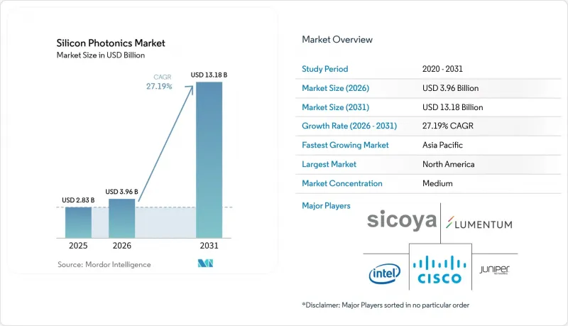
This report is Segmented by Product (Optical Switches, and More), Component (Active Components, and Passive Components), Wafer Size (300 Mm, 200 Mm, and More), Data Rate (200 Gbps, 400 Gbps, and More), Application (Telecommunications, Quantum Computing, and More), End-User (Hyperscale Cloud Providers, Telecom Operators, and More), and Geography. The Market Forecasts are Provided in Terms of Value (USD).
Global Silicon Photonics Market Trends and Insights
Energy-Efficient Co-Packaged Optics Adoption in Hyperscale Data Centers
Photonic dies are now bonded to switch silicon, removing the thermal penalties of pluggable optics and freeing valuable faceplate real estate. Marvell's 51.2 Tbps platform employs micro-ring modulators delivering 200 Gbps per lane, lowering switch power by roughly 30%. NVIDIA and TSMC use advanced interposers to route optical signals among GPU chiplets, overcoming the electrical bandwidth ceiling at 224 Gbps. Fabrinet expanded its optical module capacity by USD 132.5 million to meet swelling demand for co-packaged optics. Although the Optical Internetworking Forum released draft guidance, each hyperscaler continues to pursue proprietary form factors, fragmenting supply and complicating vendor qualification.
Carbon-Reduction Mandates Driving Low-Power Optical Interconnects
Global regulators are tightening power-use limits amid data centers' 460 TWh consumption in 2024. Silicon photonics reduces interconnect energy consumption, enabling denser racks and higher inlet temperatures. The International Energy Agency warns electricity demand could double by 2030 without optical upgrades. Omdia forecasts USD 545 billion in AI-centric capital outlays by 2030, much of it channeled to energy-efficient links. Although photonic chip fabrication is energy-intensive, lifecycle analyses still favor optics over copper for hyperscale deployments.
Thermal Budget Limitations in Silicon Substrates Above 70 °C
Ring resonators drift 0.1 nm per °C, forcing closed-loop heaters and raising module power. Automotive ambient temperatures often exceed 85 °C, demanding costly cooling or derating. Data centers mitigate with liquid loops, yet added infrastructure inflates TCO. Researchers are exploring silicon carbide and aluminum nitride substrates to potentially reduce thermo-optic coefficients, yet widespread commercial adoption is still years off.
Other drivers and restraints analyzed in the detailed report include:
- 5G Fronthaul/Backhaul Upgrade Fueling 400 G and 800 G Modules
- Automotive Level-3 LiDAR Programs Leveraging FMCW Silicon Photonics
- Lack of Standardized Packaging Elevating NRE Costs
For complete list of drivers and restraints, kindly check the Table Of Contents.
Segment Analysis
Transceivers accounted for the largest share of the silicon photonics market, holding 47.64% in 2025, propelled by hyperscale adoption of 400 G and 800 G optics. Sensors, while smaller, will post the fastest 28.74% CAGR thanks to FMCW LiDAR and refractive index biosensing. Many switch vendors are eyeing on-board lasers, suggesting some standalone transceiver volumes may migrate onto ASIC packages. Active optical cables cater to AI clusters that cannot tolerate the bulk of copper, while optical switches remain hampered by control-plane complexity.
The rise of biosensing and automotive applications signals diversification across the Photonics industry beyond telecom. Aurora's FMCW LiDAR showcases centimeter-level accuracy at 300 m range, a feat that relies on wafer-scale silicon photonics integration. In pharma, resonant-shift sensors speed high-throughput assays without fluorescent dyes, opening new licensing revenue for chip suppliers. DARPA's PIPES program is funding all-optical packet switching, suggesting optical routers could eventually disrupt electrical fabrics.
Active devices accounted for 58.91% of the silicon photonics market share in 2025 and are projected to expand at a 27.56% CAGR. Lasers remain the costliest part because silicon's indirect bandgap necessitates bonded III-V gain layers. Recent lab work demonstrated quantum-dot lasers monolithically grown on silicon, a leap that could slash the bill of materials once commercialized. Modulator bandwidth has climbed to 200 Gbps per lane using PAM4, enabling upcoming 1.6 Tbps pluggables.
Passive components, while essential, are witnessing a slower growth trajectory. Their yield is contingent on waveguide roughness and alignment tolerances, where even a single defect can jeopardize die performance. Proposals by OIF to standardize grating-coupler specifications could potentially reduce iteration cycles. With GPU vendors increasingly adopting co-packaged optics, the laser attachment process is transitioning from module houses to OSAT providers, effectively reshaping the supply chain landscape.
Complete Report Scope:
- By Product
- Optical Transceivers
- Optical Switches
- Active Optical Cables (AOCs)
- Silicon Photonic Sensors
- Wafer-Level Test Systems
- Multiplexers/De-Multiplexers
- Attenuators and Modulators
- Other Products
- By Component
- Active Components
- Lasers
- Modulators
- Photodetectors
- Passive Components
- Waveguides
- Filters
- Couplers
- Other Passive Components
- Active Components
- By Wafer Size
- 300 mm
- 200 mm
- 150 mm and Below
- By Data Rate
- Above 100 Gbps
- 200 Gbps
- 400 Gbps
- 800 Gbps
- Above 1.6 Tbps
- By Application
- Data Centers and High-Performance Computing
- Telecommunications
- Automotive and Autonomous Vehicles
- AR/VR and Consumer Electronics
- Healthcare and Life Sciences
- Defense and Aerospace
- Quantum Computing
- Other Applications
- By End-User
- Hyperscale Cloud Providers
- Telecom Operators
- Automotive OEMs and Tier-1 Suppliers
- Medical Device Manufacturers
- Government and Defense Agencies
- Research and Academic Institutions
- By Geography
- North America
- United States
- Canada
- Mexico
- Europe
- Germany
- United Kingdom
- France
- Italy
- Rest of Europe
- Asia-Pacific
- China
- Japan
- India
- South Korea
- Australia
- Rest of Asia-Pacific
- Middle East and Africa
- Middle East
- Saudi Arabia
- United Arab Emirates
- Rest of Middle East
- Africa
- South Africa
- Egypt
- Rest of Africa
- Middle East
- South America
- Brazil
- Argentina
- Rest of South America
- North America
Geography Analysis
North America held a 42.76% share in 2025, buoyed by CHIPS Act funding and vertically integrated giants such as Intel, Cisco, and Broadcom. Local access to hyperscale customers enables fast co-design cycles, while DARPA grants spur photonic packet-switching R&D. While high labor costs and lengthy permitting processes can delay fab builds, fiscal incentives significantly alleviate this burden by reducing the financial strain on companies. These incentives often include tax breaks, grants, and subsidies, which help offset the challenges associated with high operational expenses and regulatory delays.
Asia-Pacific will post the quickest 28.11% CAGR through 2031. TSMC's advanced packaging nodes enable chiplets containing photonics, logic, and memory to coexist on a single substrate, reducing interconnect power consumption. China's Made in China 2025 plan allocates billions to fab construction, aiming to localize supply and mitigate export-control risk. Japan's optics expertise and Korea's 5G rollouts also underpin demand. Geopolitical frictions, however, threaten cross-border equipment flows and IP licensing.
Europe benefits from the EUR 43 billion EU Chips Act, yet fragmentation across member states impedes scale. Germany's Fraunhofer institutes lead automotive LiDAR integration, while France's CEA-Leti partners with foundries to build pilot lines. Automotive carbon mandates and data-sovereignty rules create pull for energy-efficient photonics, although higher energy and labor costs erode manufacturing competitiveness. The Middle East and Africa, plus South America, remain early adopters, chiefly in telecom backbones upgrading to 400 G.
- Intel Corporation
- Cisco Systems Inc.
- Broadcom Inc.
- Lumentum Holdings Inc.
- Juniper Networks Inc.
- GlobalFoundries Inc.
- Sicoya GmbH
- Molex LLC
- Marvell Technology Inc.
- MACOM Technology Solutions
- Coherent Corp.
- Hamamatsu Photonics K.K.
- Ayar Labs Inc.
- NeoPhotonics Corp.
- IBM Corporation
- Hewlett Packard Enterprise Company
- Coherent Corp.
- Rockley Photonics
- Infinera Corporation
- Smart Photonics
- DustPhotonics Inc.
- PsiQuantum, Corp.
- POET Technologies
- Tower Semiconductor Ltd.
Additional Benefits:
- The market estimate (ME) sheet in Excel format
- 3 months of analyst support
TABLE OF CONTENTS
1 INTRODUCTION
- 1.1 Study Assumptions and Market Definition
- 1.2 Scope of the Study
2 RESEARCH METHODOLOGY
3 EXECUTIVE SUMMARY
4 MARKET LANDSCAPE
- 4.1 Market Overview
- 4.2 Market Drivers
- 4.2.1 Energy-Efficient Co-Packaged Optics Adoption in Hyperscale Data Centers
- 4.2.2 Carbon-Reduction Mandates Driving Low-Power Optical Interconnects
- 4.2.3 5G Fronthaul/Backhaul Upgrade Fueling 400/800 G Modules
- 4.2.4 Automotive Level-3 LiDAR Programs Leveraging FMCW Silicon Photonics
- 4.2.5 Defense Funding for Quantum and Secure Photonics
- 4.2.6 Government Semiconductor Incentive Schemes Expanding Photonic Fabs
- 4.3 Market Restraints
- 4.3.1 Thermal Budget Limitations in Silicon Substrates Above 70 °C
- 4.3.2 Lack of Standardized Packaging Elevating NRE Costs
- 4.3.3 Competition from InP and Polymer Photonics Beyond 1.55 µm
- 4.3.4 Limited 300 mm Photonic Foundry Capacity Causing Extended Lead Times
- 4.4 Industry Value Chain Analysis
- 4.5 Regulatory Outlook
- 4.6 Technological Outlook
- 4.7 Impact of Macroeconomic Factors on the Market
- 4.8 Porter's Five Forces Analysis
- 4.8.1 Bargaining Power of Suppliers
- 4.8.2 Bargaining Power of Buyers
- 4.8.3 Threat of New Entrants
- 4.8.4 Threat of Substitutes
- 4.8.5 Intensity of Competitive Rivalry
5 MARKET SIZE AND GROWTH FORECASTS (VALUE)
- 5.1 By Product
- 5.1.1 Optical Transceivers
- 5.1.2 Optical Switches
- 5.1.3 Active Optical Cables (AOCs)
- 5.1.4 Silicon Photonic Sensors
- 5.1.5 Wafer-Level Test Systems
- 5.1.6 Multiplexers/De-Multiplexers
- 5.1.7 Attenuators and Modulators
- 5.1.8 Other Products
- 5.2 By Component
- 5.2.1 Active Components
- 5.2.1.1 Lasers
- 5.2.1.2 Modulators
- 5.2.1.3 Photodetectors
- 5.2.2 Passive Components
- 5.2.2.1 Waveguides
- 5.2.2.2 Filters
- 5.2.2.3 Couplers
- 5.2.2.4 Other Passive Components
- 5.2.1 Active Components
- 5.3 By Wafer Size
- 5.3.1 300 mm
- 5.3.2 200 mm
- 5.3.3 150 mm and Below
- 5.4 By Data Rate
- 5.4.1 Above 100 Gbps
- 5.4.2 200 Gbps
- 5.4.3 400 Gbps
- 5.4.4 800 Gbps
- 5.4.5 Above 1.6 Tbps
- 5.5 By Application
- 5.5.1 Data Centers and High-Performance Computing
- 5.5.2 Telecommunications
- 5.5.3 Automotive and Autonomous Vehicles
- 5.5.4 AR/VR and Consumer Electronics
- 5.5.5 Healthcare and Life Sciences
- 5.5.6 Defense and Aerospace
- 5.5.7 Quantum Computing
- 5.5.8 Other Applications
- 5.6 By End-User
- 5.6.1 Hyperscale Cloud Providers
- 5.6.2 Telecom Operators
- 5.6.3 Automotive OEMs and Tier-1 Suppliers
- 5.6.4 Medical Device Manufacturers
- 5.6.5 Government and Defense Agencies
- 5.6.6 Research and Academic Institutions
- 5.7 By Geography
- 5.7.1 North America
- 5.7.1.1 United States
- 5.7.1.2 Canada
- 5.7.1.3 Mexico
- 5.7.2 Europe
- 5.7.2.1 Germany
- 5.7.2.2 United Kingdom
- 5.7.2.3 France
- 5.7.2.4 Italy
- 5.7.2.5 Rest of Europe
- 5.7.3 Asia-Pacific
- 5.7.3.1 China
- 5.7.3.2 Japan
- 5.7.3.3 India
- 5.7.3.4 South Korea
- 5.7.3.5 Australia
- 5.7.3.6 Rest of Asia-Pacific
- 5.7.4 Middle East and Africa
- 5.7.4.1 Middle East
- 5.7.4.1.1 Saudi Arabia
- 5.7.4.1.2 United Arab Emirates
- 5.7.4.1.3 Rest of Middle East
- 5.7.4.2 Africa
- 5.7.4.2.1 South Africa
- 5.7.4.2.2 Egypt
- 5.7.4.2.3 Rest of Africa
- 5.7.4.1 Middle East
- 5.7.5 South America
- 5.7.5.1 Brazil
- 5.7.5.2 Argentina
- 5.7.5.3 Rest of South America
- 5.7.1 North America
6 COMPETITIVE LANDSCAPE
- 6.1 Market Concentration
- 6.2 Strategic Moves
- 6.3 Market Share Analysis
- 6.4 Company Profiles (includes Global level Overview, Market level overview, Core Segments, Financials as available, Strategic Information, Market Rank/Share for key companies, Products and Services, and Recent Developments)
- 6.4.1 Intel Corporation
- 6.4.2 Cisco Systems Inc.
- 6.4.3 Broadcom Inc.
- 6.4.4 Lumentum Holdings Inc.
- 6.4.5 Juniper Networks Inc.
- 6.4.6 GlobalFoundries Inc.
- 6.4.7 Sicoya GmbH
- 6.4.8 Molex LLC
- 6.4.9 Marvell Technology Inc.
- 6.4.10 MACOM Technology Solutions
- 6.4.11 Coherent Corp.
- 6.4.12 Hamamatsu Photonics K.K.
- 6.4.13 Ayar Labs Inc.
- 6.4.14 NeoPhotonics Corp.
- 6.4.15 IBM Corporation
- 6.4.16 Hewlett Packard Enterprise Company
- 6.4.17 Coherent Corp.
- 6.4.18 Rockley Photonics
- 6.4.19 Infinera Corporation
- 6.4.20 Smart Photonics
- 6.4.21 DustPhotonics Inc.
- 6.4.22 PsiQuantum, Corp.
- 6.4.23 POET Technologies
- 6.4.24 Tower Semiconductor Ltd.
7 MARKET OPPORTUNITIES AND FUTURE OUTLOOK
- 7.1 White-space and Unmet-Need Assessment

