PUBLISHER: Mordor Intelligence | PRODUCT CODE: 2120299

PUBLISHER: Mordor Intelligence | PRODUCT CODE: 2120299
Hybrid Memory Cube - Market Share Analysis, Industry Trends & Statistics, Growth Forecasts (2026 - 2031)
According to Mordor Intelligence, the hybrid memory cube market size is expected to grow from USD 2.25 billion in 2025 to USD 2.65 billion in 2026 and is forecast to reach USD 5.99 billion by 2031 at 17.73% CAGR over 2026-2031.
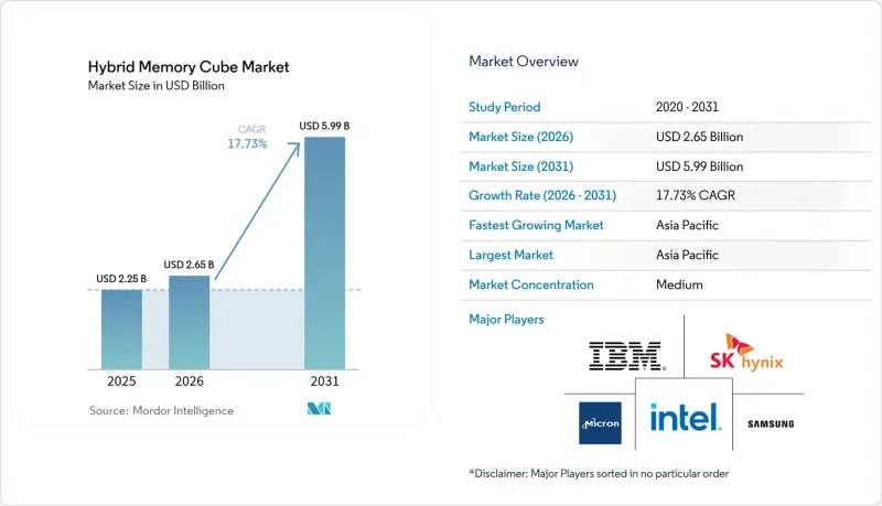
This report is Segmented by End-User Industry (Enterprise Storage, Automotive ADAS, and More), Memory Capacity (2 GB To 8 GB, 8 GB To 16 GB, 16 GB To 32 GB, Greater Than 32 GB), Application (Processor Cache, Data Buffer, Graphics Memory, Industrial and IoT Edge), Technology Node (Optical-Interconnect HMC, Chiplet-Based HMC, and More), and Geography. The Market Forecasts are Provided in Terms of Value (USD).
Global Hybrid Memory Cube Market Trends and Insights
Rapid Uptake of AI and HPC Workloads Demanding High-Bandwidth Memory
Large-language-model training has underscored the memory wall, where compute stalls before arithmetic units saturate, and Hybrid Memory Cube packages deliver up to 320 GB/s to keep GPUs and tensor cores fed. Edge inference for real-time language translation and autonomous perception now mandates low-latency DRAM alternatives, cementing demand for vertically stacked memory. Micron reported that AI server memory content doubled relative to traditional enterprise nodes in fiscal 2024, with high-bandwidth products capturing a rising percentage mix. IEEE research has found that 3-D interconnects lower energy per bit by 40% compared to DDR5, thereby reducing operating costs in megawatt-scale clusters. Continuous fine-tuning and retrieval-augmented generation extend memory footprints beyond terabyte levels, and modular scalability makes Hybrid Memory Cube attractive for such regimes. Early adopters also note latency determinism advantages, which improve quality-of-service metrics for conversational AI workloads.
Growing Enterprise Storage and Hyperscale Datacenter Refresh Cycles
Hyperscalers are replacing HDD arrays with all-flash nodes that integrate computational storage processors, and these chips demand bandwidth to manage parallel NAND channels with minimal queue depth. Intel highlighted that next-generation storage controllers rely on high-bandwidth memory to accelerate inline deduplication, erasure coding, and encryption. Enterprise refresh cycles are compressing as organizations adopt composable infrastructure, further emphasizing the need for packet-based memory interfaces that Hybrid Memory Cube supports. Samsung disclosed that enterprise SSD attach rates for stacked memory doubled year-over-year in 2024, reflecting this migration. Regulatory frameworks such as ISO 27001 intensify bandwidth needs by requiring always-on encryption and audit logging. Hyperscale operators also seek ways to reduce total rack count, and high-bandwidth memory reduces per-node latency, enabling denser deployments.
High Manufacturing Cost and TSV Yield Constraints
Deep reactive-ion etching for TSVs introduces defect mechanisms not present in planar DRAM, increasing the per-gigabyte cost by up to 60% relative to DDR5, according to SK hynix's 2024 earnings call. Yields under 85% create redundancy overhead and inflate die area, reducing gross margins. Copper-pumping failures during thermal cycling further damage bond integrity, worsening scrap rates in advanced packaging lines. Each TSV-capable cleanroom retrofit costs at least USD 500 million and needs nearly two years to qualify, limiting rapid capacity expansion. Environmental directives such as the EU's RoHS add material-substitution requirements, complicating process chemistry and further delaying scale-up. Until yield climbs above 90%, vendors are likely to focus on premium niches rather than mass-market volumes.
Other drivers and restraints analyzed in the detailed report include:
- Government-Backed Exascale Computing Initiatives in the United States, China, and Europe
- Chiplet-Based Heterogeneous Integration Architectures Gaining Traction
- Strong Incumbency of Conventional DDRx and LPDDR Technology
For complete list of drivers and restraints, kindly check the Table Of Contents.
Segment Analysis
Enterprise storage contributed 40.75% of 2025 revenue, underpinned by hyperscale operators refreshing all-flash arrays with memory-semantic storage controllers. These upgrades increase random-access throughput and use Hybrid Memory Cube packages to maintain low tail latency across parallel NAND channels. Automotive ADAS workloads, centered on Level 3 and Level 4 autonomy, are projected to rise at a 20.42% CAGR through 2031 as sensor fusion and in-vehicle AI become mainstream. Telecommunications, high-performance computing, and industrial automation each adopt the Hybrid Memory Cube to address deterministic latency needs that outstrip those of conventional DRAM. Regulatory requirements surrounding functional-safety certification and cybersecurity accelerate procurement in safety-critical domains.
Automotive growth highlights the shift of the hybrid memory cube market toward edge devices, which prioritize thermal efficiency and sustained bandwidth. The sensor count per vehicle is climbing, and real-time perception algorithms benefit directly from low-latency memory. Enterprise storage growth is now moderating as penetration reaches mature levels in North America and Europe, though ongoing capacity optimization ensures continued product cycles. Telecommunications operators are leveraging pooled-memory constructs in 5G core deployments. Government policies, such as the FCC's Open RAN push and the EU Machinery Regulation, also champion modular memory architectures that Hybrid Memory Cube supports.
Modules in the 16 GB to 32 GB range captured 37.15% of 2025 deployments, aligning with expectations for dual-socket servers and providing the optimal sweet spot for cost-performance balance. The hybrid memory cube market size for capacities greater than 32 GB is forecast to expand at a 19.62% CAGR as large-language-model inference nodes and NUMA systems deploy multi-terabyte pools. The 8 GB-to-16 GB tier supports power-constrained edge servers, while devices with capacities below 8 GB remain common in embedded industrial controls, where radiation tolerance and extended temperature ratings take precedence over raw capacity.
The average memory per socket has doubled from 128 GB in 2020 to 256 GB in 2024, and the shift toward AI inference servers that store model weights in system memory has widened the addressable high-capacity segment. Network-slice orchestration functions in 5G cores further raise per-node capacity needs. Functional-safety and cybersecurity standards effectively double usable memory to accommodate redundancy and parity, reinforcing the case for moving up to larger HMC packages in control-plane equipment.
Complete Report Scope:
- By End-User Industry
- Enterprise Storage
- Telecommunications and Networking
- High-Performance Computing
- Automotive ADAS
- Other End-User Industry
- By Memory Capacity
- 2 GB-8 GB
- 8 GB-16 GB
- 16 GB-32 GB
- Above 32 GB
- By Application
- Processor Cache
- Data Buffer
- Graphics Memory
- Industrial / IoT Edge
- By Technology Node
- TSV-based Hybrid Memory Cube (Gen 2)
- Optical-interconnect HMC
- Chiplet-based HMC
- By Geography
- North America
- United States
- Canada
- Mexico
- South America
- Brazil
- Argentina
- Rest of South America
- Europe
- Germany
- United Kingdom
- France
- Italy
- Spain
- Russia
- Rest of Europe
- Asia Pacific
- China
- Japan
- India
- South Korea
- Australia
- Rest of Asia Pacific
- Middle East and Africa
- Middle East
- Saudi Arabia
- United Arab Emirates
- Turkey
- Rest of Middle East
- Africa
- South Africa
- Nigeria
- Egypt
- Rest of Africa
- Middle East
- North America
Geography Analysis
The Asia Pacific delivered 41.05% of the hybrid memory cube market revenue in 2025 and is projected to grow at a 19.93% CAGR to 2031, driven by concentrated fabrication capacity at Samsung and SK hynix, as well as pro-semiconductor policies in China, Japan, South Korea, and India. The Chinese government's funds, totaling CNY 15 billion in 2024, target domestic stacked-memory innovation, while Japanese co-investment supports chiplet packaging through 2-nm nodes. Indian hyperscalers are drafting regional language AI models that require high-bandwidth memory, advancing in-country demand. Taiwan's wafer-level packaging expansions further anchor the region as a hub for heterogeneous integration services.
North America represented 28.35% of 2025 revenue, driven by hyperscale cloud refresh cycles and the Department of Energy's exascale programs. Intel's USD 20 billion Ohio expansion will house advanced packaging lines to embed Hybrid Memory Cube dies directly into Xeon and GPU assemblies. Amazon Web Services, Microsoft Azure, and Google Cloud all pilot disaggregated memory fabrics that pool high-bandwidth tiers across racks, a model that maximizes utilization while controlling per-server costs. Canada's Vector and Mila institutes deploy HMC-based clusters to underpin national AI research goals. Export controls restricting advanced memory shipments reshape supply allocation patterns and drive onshore capacity investments.
Europe captured approximately 17.65% of the 2025 revenue, driven by the adoption of automotive ADAS and the installation of EuroHPC supercomputers. German tier-ones Bosch and Continental incorporated Hybrid Memory Cube into Level 3 perception platforms to meet stringent latency budgets. The region's sovereign cloud push requires GDPR-compliant configurations, which in turn need encryption-friendly memory architectures. Arm expanded a coherent interconnect IP portfolio in 2024 to support European automotive and edge customers, underscoring local R&D momentum. The EU Chips Act funnels EUR 43 billion to double the regional semiconductor share, part of which finances advanced packaging for stacked memory lines.
- Micron Technology Inc.
- Intel Corporation
- Samsung Electronics Co., Ltd.
- SK hynix Inc.
- International Business Machines Corporation
- Advanced Micro Devices Inc.
- Xilinx, Inc.
- Fujitsu Ltd.
- Marvell Technology, Inc.
- Rambus Inc.
- Broadcom Inc.
- Cadence Design Systems Inc.
- ASE Technology Holding Co., Ltd.
- Semtech Corporation
- Open-Silicon, Inc.
- Arm Ltd.
- Altera Corporation (Intel PSG)
- Taiwan Semiconductor Manufacturing Company Ltd.
- Hitachi Ltd.
- Renesas Electronics Corporation
Additional Benefits:
- The market estimate (ME) sheet in Excel format
- 3 months of analyst support
TABLE OF CONTENTS
1 INTRODUCTION
- 1.1 Study Assumptions and Market Definition
- 1.2 Scope of the Study
2 RESEARCH METHODOLOGY
3 EXECUTIVE SUMMARY
4 MARKET LANDSCAPE
- 4.1 Market Overview
- 4.2 Market Drivers
- 4.2.1 Growing Enterprise Storage and Hyperscale Datacenter Refresh Cycles
- 4.2.2 Rapid Uptake Of AI / HPC Workloads Demanding High-Bandwidth Memory
- 4.2.3 Expanding 5G Core and Edge Networking Equipment Deployments
- 4.2.4 Government-Backed Exascale Computing Initiatives in the United States, China And Europe
- 4.2.5 Chiplet-Based Heterogeneous Integration Architectures Gaining Traction
- 4.2.6 Shift Toward Composable and Disaggregated Server Architecture in Cloud Platforms
- 4.3 Market Restraints
- 4.3.1 Strong Incumbency of Conventional Ddrx / LPDDR DRAM Technology
- 4.3.2 High Manufacturing Cost and TSV Yield Constraints
- 4.3.3 Thermal Management Complexity In 3-D Stacked Memory Cubes
- 4.3.4 Limited Supplier Ecosystem and IP Licensing Frictions
- 4.4 Industry Value Chain Analysis
- 4.5 Impact of Macroeconomic Factors
- 4.6 Regulatory Landscape
- 4.7 Technological Outlook
- 4.8 Porter's Five Forces Analysis
- 4.8.1 Bargaining Power of Buyers
- 4.8.2 Bargaining Power of Suppliers
- 4.8.3 Threat of New Entrants
- 4.8.4 Threat of Substitute Products
- 4.8.5 Intensity of Competitive Rivalry
5 MARKET SIZE AND GROWTH FORECASTS (VALUE)
- 5.1 By End-User Industry
- 5.1.1 Enterprise Storage
- 5.1.2 Telecommunications and Networking
- 5.1.3 High-Performance Computing
- 5.1.4 Automotive ADAS
- 5.1.5 Other End-User Industry
- 5.2 By Memory Capacity
- 5.2.1 2 GB-8 GB
- 5.2.2 8 GB-16 GB
- 5.2.3 16 GB-32 GB
- 5.2.4 Above 32 GB
- 5.3 By Application
- 5.3.1 Processor Cache
- 5.3.2 Data Buffer
- 5.3.3 Graphics Memory
- 5.3.4 Industrial / IoT Edge
- 5.4 By Technology Node
- 5.4.1 TSV-based Hybrid Memory Cube (Gen 2)
- 5.4.2 Optical-interconnect HMC
- 5.4.3 Chiplet-based HMC
- 5.5 By Geography
- 5.5.1 North America
- 5.5.1.1 United States
- 5.5.1.2 Canada
- 5.5.1.3 Mexico
- 5.5.2 South America
- 5.5.2.1 Brazil
- 5.5.2.2 Argentina
- 5.5.2.3 Rest of South America
- 5.5.3 Europe
- 5.5.3.1 Germany
- 5.5.3.2 United Kingdom
- 5.5.3.3 France
- 5.5.3.4 Italy
- 5.5.3.5 Spain
- 5.5.3.6 Russia
- 5.5.3.7 Rest of Europe
- 5.5.4 Asia Pacific
- 5.5.4.1 China
- 5.5.4.2 Japan
- 5.5.4.3 India
- 5.5.4.4 South Korea
- 5.5.4.5 Australia
- 5.5.4.6 Rest of Asia Pacific
- 5.5.5 Middle East and Africa
- 5.5.5.1 Middle East
- 5.5.5.1.1 Saudi Arabia
- 5.5.5.1.2 United Arab Emirates
- 5.5.5.1.3 Turkey
- 5.5.5.1.4 Rest of Middle East
- 5.5.5.2 Africa
- 5.5.5.2.1 South Africa
- 5.5.5.2.2 Nigeria
- 5.5.5.2.3 Egypt
- 5.5.5.2.4 Rest of Africa
- 5.5.5.1 Middle East
- 5.5.1 North America
6 COMPETITIVE LANDSCAPE
- 6.1 Market Concentration
- 6.2 Strategic Moves
- 6.3 Market Share Analysis
- 6.4 Company Profiles (includes Global level Overview, Market level overview, Core Segments, Financials as available, Strategic Information, Market Rank / Share for key companies, Products and Services, and Recent Developments)
- 6.4.1 Micron Technology Inc.
- 6.4.2 Intel Corporation
- 6.4.3 Samsung Electronics Co., Ltd.
- 6.4.4 SK hynix Inc.
- 6.4.5 International Business Machines Corporation
- 6.4.6 Advanced Micro Devices Inc.
- 6.4.7 Xilinx, Inc.
- 6.4.8 Fujitsu Ltd.
- 6.4.9 Marvell Technology, Inc.
- 6.4.10 Rambus Inc.
- 6.4.11 Broadcom Inc.
- 6.4.12 Cadence Design Systems Inc.
- 6.4.13 ASE Technology Holding Co., Ltd.
- 6.4.14 Semtech Corporation
- 6.4.15 Open-Silicon, Inc.
- 6.4.16 Arm Ltd.
- 6.4.17 Altera Corporation (Intel PSG)
- 6.4.18 Taiwan Semiconductor Manufacturing Company Ltd.
- 6.4.19 Hitachi Ltd.
- 6.4.20 Renesas Electronics Corporation
7 MARKET OPPORTUNITIES AND FUTURE OUTLOOK
- 7.1 White-space and Unmet-need Assessment

