PUBLISHER: Mordor Intelligence | PRODUCT CODE: 2121739

PUBLISHER: Mordor Intelligence | PRODUCT CODE: 2121739
Microscopy Device - Market Share Analysis, Industry Trends & Statistics, Growth Forecasts (2026 - 2031)
According to Mordor Intelligence, the microscopy device market size is projected to be USD 10.23 billion in 2025, USD 10.82 billion in 2026, and reach USD 14.32 billion by 2031, growing at a CAGR of 5.76% from 2026 to 2031.
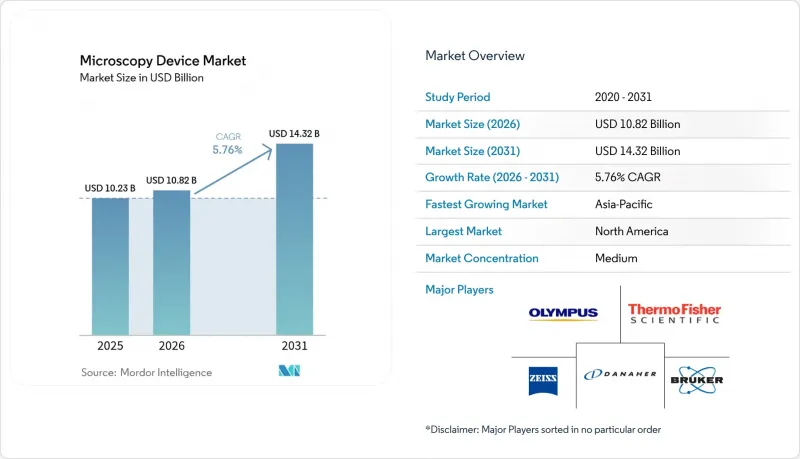
This report is Segmented by Microscopy Type (Electron Microscopy, Optical Microscopy, Scanning Probe Microscopy, Other Technologies), Application (Nanotechnology Research, Life Science, Semiconductor & Electronics, and More), End User (Hospitals, Clinics and Diagnostic Labs, and More), and Geography (North America, Europe, Asia-Pacific, and More). The Market Forecasts are Provided in Terms of Value (USD).
Global Microscopy Device Market Trends and Insights
Technological Advancements in Super-Resolution Optics & Quantum Sensing
Super-resolution techniques like STED, SIM, and PALM are breaking the diffraction barrier to reveal structures below 50 nanometers, which strengthens single-cell and neurodegeneration research as labs push to quantify protein interactions in living systems. Early adopters are layering quantum sensing based on nitrogen-vacancy centers in diamond to image magnetic fields, detect nanoscale defects in semiconductor wafers, and capture single-molecule events in biophysics. The microscopy device market is benefiting as buyers seek hybrid platforms that switch among widefield, confocal, and super-resolution modes within the same workflow to maximize throughput. Academic consortia and pharmaceutical companies in North America and Europe are leading purchases due to pipeline demands for target validation and high-content screening. Complexity in optical alignment and reliance on specific fluorophores still slow routine clinical use, creating a service and training opportunity for vendors with robust application support.
AI-Driven Automated Digital Pathology Adoption
Pathology networks are moving from manual microscopy to whole-slide imaging combined with convolutional neural networks that classify tissue, quantify biomarkers, and flag anomalies, and several models now show sensitivities exceeding 95% in indications with strong ground truth. In January 2026, the Central Silk Board in India highlighted an AI-enabled microscope initiative that helps farmers detect silkworm disease earlier, underscoring how applied AI microscopy is expanding beyond clinical settings into production environments. Oncology workloads are a catalyst because tumor microenvironment analysis requires quantifying immune infiltrates and vascular structures across gigapixel images at scale. The European Union's In Vitro Diagnostic Regulation mandates CE marking for AI-based diagnostic software, prompting vendors to run prospective clinical validation studies to align model performance with clinical endpoints. Hospitals and diagnostic labs are the fastest-growing end-user segment at a 6.60% CAGR through 2031, driven by pathologist labor constraints and the need to standardize multi-site interpretations to reduce variability in care
High Capital & Operating Costs of Devices
The upfront cost of high-end cryo-EM suites remains in the USD 5 million to USD 7 million range once facilities, shielding, and vibration isolation are included, and this delays access for many centers that depend on pooled grants. Annual operating expenses for aberration-corrected TEMs can reach USD 200,000, including maintenance, cryogens, and cleanroom utilities, which limits broader adoption even when equipment is partially subsidized. Shared-facility and leasing models soften the barrier, but scheduling, maintenance windows, and variable uptime add coordination costs for multi-institution use. For hospitals and diagnostic labs, budget ceilings slow digital pathology deployments even where throughput and standardization gains support a clear business case. The microscopy device market reflects these capital constraints in emerging economies, where currency risk and import duties add further headwinds to large-ticket equipment purchases.
Other drivers and restraints analyzed in the detailed report include:
- Government Nanotech & Life-Science R&D Funding Surge
- Semiconductor Gate-All-Around Node Miniaturization Needs
- Global Shortage of Hybrid Optics-Software Talent
For complete list of drivers and restraints, kindly check the Table Of Contents.
Segment Analysis
Electron microscopy is forecast to grow at 6.56% annually from 2026 to 2031, outpacing the broader microscopy device market, driven by compact cryo-EM systems. Adoption rises when structure-based drug design workflows require higher throughput and local control over sample preparation and data processing to shorten iteration cycles. In parallel, semiconductor fabs are increasing TEM and SEM tool counts to inspect nanosheet stacks, spacers, and hidden defects that are not visible with optical metrology at 2-nanometer-class nodes. Aberration-corrected optics and advanced detectors remain the differentiators for lattice-strain mapping and atomic-column resolution during logic and memory ramps. These factors are pushing electron platforms into a larger role across both process development and failure analysis as fabs seek greater statistical coverage and reliability in metrology.
Optical microscopy commanded 41.80% of % microscopy device market share in 2025, given its ubiquity in clinical workflows, teaching labs, and quality control environments that value ease of use and lower service overheads.
Complete Report Scope:
- By Microscopy Type
- Electron Microscopy
- Transmission Electron Microscopy (TEM)
- Scanning Electron Microscopy (SEM)
- Cryogenic Electron Microscopy (Cryo-EM)
- Optical Microscopy
- Bright-field & Phase-contrast
- Fluorescence & Confocal
- Super-resolution (STED, SIM, PALM)
- Scanning Probe Microscopy
- Atomic Force Microscopy (AFM)
- Scanning Tunneling Microscopy (STM)
- Other Technologies
- Electron Microscopy
- By Application
- Life Science
- Nanotechnology Research
- Semiconductor & Electronics
- Materials Science & Metallurgy
- Other Applications
- By End User
- Academic & Research Institutes
- Hospitals, Clinics & Diagnostic Labs
- Pharmaceutical & Biotechnology Companies
- Semiconductor & Electronics Manufacturers
- Others
- By Geography
- North America
- United States
- Canada
- Mexico
- Europe
- Germany
- United Kingdom
- France
- Italy
- Spain
- Rest of Europe
- Asia-Pacific
- China
- India
- Japan
- Australia
- South Korea
- Rest of Asia-Pacific
- Middle East and Africa
- GCC
- South Africa
- Rest of Middle East and Africa
- South America
- Brazil
- Argentina
- Rest of South America
- North America
Geography Analysis
North America commanded 39.25% of the microscopy device market share in 2025, as pharma R&D, academic research output, and semiconductor investments supported sustained procurement of optical and electron microscopy platforms. The CHIPS and Science Act allocates USD 52.7 billion across manufacturing incentives and research programs, which elevates demand for advanced metrology fleets at Intel and other operators building new lines in Arizona and Ohio. University labs in the United States and Canada continue to purchase cryo-EM and super-resolution systems with support from national programs that expanded in 2025, including Canada's Strategic Innovation Fund, which allocated CAD 450 million (USD 335 million) to research infrastructure. These factors anchor a stable replacement cycle and add new first-time buyers as hospitals scale digital pathology and standardize across networks. The microscopy device market in North America also benefits from a strong service ecosystem and vendor presence, which accelerates training and validation for regulated workflows.
Europe sustains a mature installed base shaped by public funding and harmonized regulations that emphasize clinical validation and sustainability. Horizon Europe committed EUR 95.5 billion (USD 102 billion) through 2027 for research and innovation, and dedicated photonics and nanomedicine streams continue to support procurement of high-end imaging platforms across universities and clinical centers.
Asia-Pacific remains the fastest-growing region, with a projected 6.74% CAGR, and the microscopy device market aligns with government programs that prioritize domestic semiconductor and life sciences capabilities. China's policy support helps local research centers and industrial labs scale adoption of electron platforms for logic, memory, and advanced materials, thereby generating consistent orders for TEM, SEM, and related accessories. Outside these hubs, the Middle East and Africa are scaling research infrastructure as part of diversification strategies. At the same time, Latin America faces budget headwinds that temper near-term growth despite active research communities.
- Ametek (Cameca)
- Andor Technology Ltd.
- Bruker
- Carl Zeiss
- Cytovale Inc.
- Danaher
- Delong Instruments
- Euromex Microscopes
- Hitachi
- JEOL Ltd.
- Keyence Corporation
- Labomed Inc.
- Motic Microscopes
- Nikon
- NTMDT
- Olympus
- Oxford Instruments (Asylum Research)
- Oxford Instruments
- Park Systems Corp.
- Tescan Orsay Holding
- Thermo Fisher Scientific
Additional Benefits:
- The market estimate (ME) sheet in Excel format
- 3 months of analyst support
TABLE OF CONTENTS
1 Introduction
- 1.1 Study Assumptions & Market Definition
- 1.2 Scope of the Study
2 Research Methodology
3 Executive Summary
4 Market Landscape
- 4.1 Market Overview
- 4.2 Market Drivers
- 4.2.1 Technological Advancements in Super-Resolution Optics & Quantum Sensing
- 4.2.2 AI-Driven Automated Digital Pathology Adoption
- 4.2.3 Government Nanotech & Life-Science R&D Funding Surge
- 4.2.4 Semiconductor Gate-All-Around Node Miniaturization Needs
- 4.2.5 Desktop Cryo-EM Democratizing Structure-Based Drug Design
- 4.2.6 Sustainability Push For Energy-Efficient, Modular Microscopes
- 4.3 Market Restraints
- 4.3.1 High Capital & Operating Costs of Devices
- 4.3.2 Global Shortage of Hybrid Optics-Software Talent
- 4.3.3 Precision-Optic Supply-Chain Bottlenecks (Germanium, Gallium)
- 4.3.4 Escalating IP-Litigation Risks in Cross-Border Tech Transfer
- 4.4 Supply-Chain Analysis
- 4.5 Regulatory Landscape
- 4.6 Technological Outlook
- 4.7 Porters Five Forces Analysis
- 4.7.1 Threat of New Entrants
- 4.7.2 Bargaining Power of Buyers
- 4.7.3 Bargaining Power of Suppliers
- 4.7.4 Threat of Substitutes
- 4.7.5 Intensity of Competitive Rivalry
5 Market Size & Growth Forecasts (Value, USD)
- 5.1 By Microscopy Type
- 5.1.1 Electron Microscopy
- 5.1.1.1 Transmission Electron Microscopy (TEM)
- 5.1.1.2 Scanning Electron Microscopy (SEM)
- 5.1.1.3 Cryogenic Electron Microscopy (Cryo-EM)
- 5.1.2 Optical Microscopy
- 5.1.2.1 Bright-field & Phase-contrast
- 5.1.2.2 Fluorescence & Confocal
- 5.1.2.3 Super-resolution (STED, SIM, PALM)
- 5.1.3 Scanning Probe Microscopy
- 5.1.3.1 Atomic Force Microscopy (AFM)
- 5.1.3.2 Scanning Tunneling Microscopy (STM)
- 5.1.4 Other Technologies
- 5.1.1 Electron Microscopy
- 5.2 By Application
- 5.2.1 Life Science
- 5.2.2 Nanotechnology Research
- 5.2.3 Semiconductor & Electronics
- 5.2.4 Materials Science & Metallurgy
- 5.2.5 Other Applications
- 5.3 By End User
- 5.3.1 Academic & Research Institutes
- 5.3.2 Hospitals, Clinics & Diagnostic Labs
- 5.3.3 Pharmaceutical & Biotechnology Companies
- 5.3.4 Semiconductor & Electronics Manufacturers
- 5.3.5 Others
- 5.4 By Geography
- 5.4.1 North America
- 5.4.1.1 United States
- 5.4.1.2 Canada
- 5.4.1.3 Mexico
- 5.4.2 Europe
- 5.4.2.1 Germany
- 5.4.2.2 United Kingdom
- 5.4.2.3 France
- 5.4.2.4 Italy
- 5.4.2.5 Spain
- 5.4.2.6 Rest of Europe
- 5.4.3 Asia-Pacific
- 5.4.3.1 China
- 5.4.3.2 India
- 5.4.3.3 Japan
- 5.4.3.4 Australia
- 5.4.3.5 South Korea
- 5.4.3.6 Rest of Asia-Pacific
- 5.4.4 Middle East and Africa
- 5.4.4.1 GCC
- 5.4.4.2 South Africa
- 5.4.4.3 Rest of Middle East and Africa
- 5.4.5 South America
- 5.4.5.1 Brazil
- 5.4.5.2 Argentina
- 5.4.5.3 Rest of South America
- 5.4.1 North America
6 Competitive Landscape
- 6.1 Market Concentration
- 6.2 Market Share Analysis
- 6.3 Company Profiles (includes Global level Overview, Market-level Overview, Core Segments, Financials, Strategic Information, Market Rank/Share, Products & Services, Recent Developments)
- 6.3.1 Ametek (Cameca)
- 6.3.2 Andor Technology Ltd.
- 6.3.3 Bruker Corporation
- 6.3.4 Carl Zeiss AG
- 6.3.5 Cytovale Inc.
- 6.3.6 Danaher Corporation (Leica Microsystems)
- 6.3.7 Delong Instruments
- 6.3.8 Euromex Microscopes
- 6.3.9 Hitachi High-Tech Corporation
- 6.3.10 JEOL Ltd.
- 6.3.11 Keyence Corporation
- 6.3.12 Labomed Inc.
- 6.3.13 Motic Microscopes
- 6.3.14 Nikon Corporation
- 6.3.15 NTMDT
- 6.3.16 Olympus Corporation
- 6.3.17 Oxford Instruments (Asylum Research)
- 6.3.18 Oxford Instruments PLC
- 6.3.19 Park Systems Corp.
- 6.3.20 Tescan Orsay Holding
- 6.3.21 Thermo Fisher Scientific Inc.
7 Market Opportunities & Future Outlook
- 7.1 White-space & Unmet-need Assessment

