PUBLISHER: Mordor Intelligence | PRODUCT CODE: 2124091

PUBLISHER: Mordor Intelligence | PRODUCT CODE: 2124091
Compound Semiconductor - Market Share Analysis, Industry Trends & Statistics, Growth Forecasts (2026 - 2031)
According to Mordor Intelligence, the compound semiconductor market size in 2026 is estimated at USD 40.02 billion, growing from 2025 value of USD 35.95 billion with 2031 projections showing USD 68.47 billion, growing at 11.32% CAGR over 2026-2031.
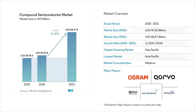
This report is Segmented by Material Type (Gallium Arsenide, Gallium Nitride, Silicon Carbide, and More), Wafer Size (<=100mm, 150mm, 200mm, and 300mm and Above), Device Type (RF and Microwave Devices, and More), End-User Industry (Telecom and Datacom Infrastructure, Consumer Electronics, Industrial and Energy, and More), and Geography (North America, Europe, Asia-Pacific, South America, Middle East and Africa).
Global Compound Semiconductor Market Trends and Insights
GaN-on-Si power devices in EU and China EV chargers
European emissions rules and China's highway electrification drove GaN-on-Si adoption in 350 kW and higher fast chargers that achieved 95% power-conversion efficiency and cut installation costs by up to 40% compared with silicon alternatives. EU Green Deal funding of EUR 2 billion (USD 2.26 billion) for wide-bandgap fabs reinforced the transition, while China's gallium export curbs spurred local sourcing strategies.
5G massive-MIMO RF front-ends in US and APAC
The migration toward standalone 5G and 64T64R or larger antenna arrays required GaAs and GaN power amplifiers that reduced base-station energy use by 40% and enabled millimeter-wave coverage. Initial deployments in South Korea reached 95% population coverage, and CHIPS Act grants prepared US fabs for domestic GaAs expansion.
Shortage of 200 mm SiC substrates
Manufacturers reported a 40% supply gap for 200 mm SiC wafers because boule growth cycles took up to 14 days, and furnace capacity was limited. Automotive OEMs, therefore, locked multi-year deals at premium prices, and substrate makers such as II-VI gained pricing power.
Other drivers and restraints analyzed in the detailed report include:
- Micro/Mini-LED adoption in TVs and AR wearables
- SiC traction inverters for European commercial EVs
- High Cap-Ex of MOCVD reactors
For complete list of drivers and restraints, kindly check the Table Of Contents.
Segment Analysis
The compound semiconductor market size for materials saw gallium arsenide retain a 46.85% share in 2025. Silicon carbide recorded an 18.1% CAGR outlook, underpinned by traction inverters and fast-charging power modules. Gallium nitride took incremental share through 650 V bidirectional IC launches that widened adoption in energy-storage bidirectional chargers. Indium phosphide remained essential in LiDAR photonic integrated circuits and sub-THz 6G prototypes, although absolute volumes were low.
Segment growth hinged on wide-bandgap attributes, high electron mobility and high breakdown voltage, that silicon could not match. Research breakthroughs in RF GaN-on-Si promised to extend GaN usage into 6G base-station PAs. Cost pressures lingered because gallium and indium feedstock remained under export-control scrutiny, raising interest in recycled sources and material alternatives such as AlYN.
In 2025, 150 mm substrates captured 48.02% revenue, yet 200 mm platforms projected the fastest 14.95% CAGR. Automotive power modules, which depend on high die counts, favoured 200 mm to secure a projected 30% die-per-wafer cost saving over 150 mm lines. Infineon's Malaysia megafab validated the scale economics with 200 mm SiC lines designed for 30% of global supply by 2030.
Smaller (<= 100 mm) formats preserved positions in low-volume, performance-critical sectors such as satellite communications. While 300 mm opportunities emerged in GaN-on-Si prototypes, technical hurdles-film stress, bow control, and defect density-kept commercial adoption beyond the forecast period. Equipment suppliers prioritised 200 mm reactor platforms to maximise utilisation, targeting 85-90% loading to amortise capital costs.
Complete Report Scope:
- By Material Type
- Gallium Arsenide (GaAs)
- Gallium Nitride (GaN)
- Silicon Carbide (SiC)
- Indium Phosphide (InP)
- Gallium Phosphide (GaP)
- Other III-V and II-VI Compounds
- By Wafer Size
- <=100 mm
- 150 mm
- 200 mm
- 300 mm and Above
- By Device Type
- Light-Emitting Diodes (LED)
- Radio-Frequency and Microwave Devices
- Optoelectronics (Laser, Photodetector)
- Power Electronics
- Photovoltaic Cells
- By End-User Industry
- Telecom and Datacom Infrastructure
- Consumer Electronics
- Automotive and Transportation
- Industrial and Energy
- Aerospace and Defense
- Healthcare and Life Sciences
- Others
- By Geography
- North America
- United States
- Canada
- Mexico
- Europe
- Germany
- United Kingdom
- France
- Italy
- Nordics (Sweden, Finland, Norway, Denmark)
- Rest of Europe
- Asia-Pacific
- China
- Japan
- South Korea
- India
- Taiwan
- Rest of Asia-Pacific
- South America
- Brazil
- Argentina
- Mexico
- Rest of South America
- Middle East and Africa
- Middle East
- Saudi Arabia
- United Arab Emirates
- Turkey
- Rest of Middle East
- Africa
- South Africa
- Rest of Africa
- Middle East
- North America
Geography Analysis
Asia-Pacific held 58.25% revenue in 2025 and posted a 13.95% CAGR outlook to 2031. The compound semiconductor market size for the region benefited from China's planned 8.6 million-wafer-per-month capacity and Taiwan's foundry dominance. Export controls on gallium, germanium, and indium introduced in 2024 highlighted concentration risks, prompting local governments to channel subsidies toward upstream materials.
North America advanced domestic supply-chain agendas under the USD 39 billion CHIPS incentive. Skyworks and Qorvo lined up GaAs expansion projects, and TSMC's USD 165 billion Arizona cluster accelerated to include compound-semiconductor advanced-packaging capability. Defense requirements for assured access to III-V devices added impetus.
Europe positioned wide-bandgap semiconductors as a pillar of its Green Deal and European Chips Act. Germany allocated EUR 2 billion (USD 2.26 billion) to local production, while Nexperia committed USD 200 million for a Hamburg SiC line. Supply-chain localisation aims to mitigate Asia-centric shocks such as the quartz-mine disruption in North Carolina that threatened 70-90% of global high-purity quartz.
- Wolfspeed Inc.
- Skyworks Solutions Inc.
- Qorvo Inc.
- Infineon Technologies AG
- STMicroelectronics N.V.
- Onsemi (Semiconductor Components Industries LLC)
- Analog Devices Inc.
- Texas Instruments Inc.
- ams-OSRAM AG
- Rohm Semiconductor
- NXP Semiconductors N.V.
- GaN Systems Inc.
- Transphorm Inc.
- MACOM Technology Solutions Holdings Inc.
- IQE plc
- Coherent Corp. (II-VI)
- WIN Semiconductors Corp.
- Advanced Wireless Semiconductor Company
- Nichia Corporation
- Epistar Corporation
- Sumitomo Electric Industries Ltd.
- Renesas Electronics Corporation
- Mitsubishi Electric Corporation
- Microchip Technology Inc.
- Veeco Instruments Inc.
Additional Benefits:
- The market estimate (ME) sheet in Excel format
- 3 months of analyst support
TABLE OF CONTENTS
1 INTRODUCTION
- 1.1 Study Assumptions and Market Definition
- 1.2 Scope of the Study
2 RESEARCH METHODOLOGY
3 EXECUTIVE SUMMARY
4 MARKET LANDSCAPE
- 4.1 Market Overview
- 4.2 Market Drivers
- 4.2.1 GaN-on-Si Power Devices in EU and China EV Chargers
- 4.2.2 5G Massive-MIMO RF Front-Ends in US and APAC
- 4.2.3 Micro/Mini-LED Adoption in TVs and AR Wearables
- 4.2.4 SiC Traction Inverters for European Commercial EVs
- 4.2.5 III-V FAB Incentives under US/EU CHIPS Acts
- 4.2.6 InP-Based LiDAR PICs for Autonomous Vehicles
- 4.3 Market Restraints
- 4.3.1 Shortage of 200 mm SiC Substrates
- 4.3.2 High Cap-Ex of MOCVD Reactors
- 4.3.3 Reliability Concerns in >650 V GaN Devices
- 4.3.4 US Export Controls on Epi Tools to China
- 4.4 Value Chain Analysis
- 4.5 Technological Outlook
- 4.6 Regulatory Outlook
- 4.7 Porter's Five Forces Analysis
- 4.7.1 Bargaining Power of Suppliers
- 4.7.2 Bargaining Power of Buyers
- 4.7.3 Threat of New Entrants
- 4.7.4 Threat of Substitutes
- 4.7.5 Intensity of Competitive Rivalry
- 4.8 Impact of Macroeconomic Trends on Compound Semiconductor Demand
5 MARKET SIZE AND GROWTH FORECASTS (VALUE)
- 5.1 By Material Type
- 5.1.1 Gallium Arsenide (GaAs)
- 5.1.2 Gallium Nitride (GaN)
- 5.1.3 Silicon Carbide (SiC)
- 5.1.4 Indium Phosphide (InP)
- 5.1.5 Gallium Phosphide (GaP)
- 5.1.6 Other III-V and II-VI Compounds
- 5.2 By Wafer Size
- 5.2.1 <=100 mm
- 5.2.2 150 mm
- 5.2.3 200 mm
- 5.2.4 300 mm and Above
- 5.3 By Device Type
- 5.3.1 Light-Emitting Diodes (LED)
- 5.3.2 Radio-Frequency and Microwave Devices
- 5.3.3 Optoelectronics (Laser, Photodetector)
- 5.3.4 Power Electronics
- 5.3.5 Photovoltaic Cells
- 5.4 By End-User Industry
- 5.4.1 Telecom and Datacom Infrastructure
- 5.4.2 Consumer Electronics
- 5.4.3 Automotive and Transportation
- 5.4.4 Industrial and Energy
- 5.4.5 Aerospace and Defense
- 5.4.6 Healthcare and Life Sciences
- 5.4.7 Others
- 5.5 By Geography
- 5.5.1 North America
- 5.5.1.1 United States
- 5.5.1.2 Canada
- 5.5.1.3 Mexico
- 5.5.2 Europe
- 5.5.2.1 Germany
- 5.5.2.2 United Kingdom
- 5.5.2.3 France
- 5.5.2.4 Italy
- 5.5.2.5 Nordics (Sweden, Finland, Norway, Denmark)
- 5.5.2.6 Rest of Europe
- 5.5.3 Asia-Pacific
- 5.5.3.1 China
- 5.5.3.2 Japan
- 5.5.3.3 South Korea
- 5.5.3.4 India
- 5.5.3.5 Taiwan
- 5.5.3.6 Rest of Asia-Pacific
- 5.5.4 South America
- 5.5.4.1 Brazil
- 5.5.4.2 Argentina
- 5.5.4.3 Mexico
- 5.5.4.4 Rest of South America
- 5.5.5 Middle East and Africa
- 5.5.5.1 Middle East
- 5.5.5.1.1 Saudi Arabia
- 5.5.5.1.2 United Arab Emirates
- 5.5.5.1.3 Turkey
- 5.5.5.1.4 Rest of Middle East
- 5.5.5.2 Africa
- 5.5.5.2.1 South Africa
- 5.5.5.2.2 Rest of Africa
- 5.5.5.1 Middle East
- 5.5.1 North America
6 COMPETITIVE LANDSCAPE
- 6.1 Market Concentration
- 6.2 Strategic Moves
- 6.3 Market Share Analysis
- 6.4 Company Profiles (includes Global-level Overview, Market-level Overview, Core Segments, Financials as available, Strategic Information, Market Rank/Share, Products and Services, Recent Developments)
- 6.4.1 Wolfspeed Inc.
- 6.4.2 Skyworks Solutions Inc.
- 6.4.3 Qorvo Inc.
- 6.4.4 Infineon Technologies AG
- 6.4.5 STMicroelectronics N.V.
- 6.4.6 Onsemi (Semiconductor Components Industries LLC)
- 6.4.7 Analog Devices Inc.
- 6.4.8 Texas Instruments Inc.
- 6.4.9 ams-OSRAM AG
- 6.4.10 Rohm Semiconductor
- 6.4.11 NXP Semiconductors N.V.
- 6.4.12 GaN Systems Inc.
- 6.4.13 Transphorm Inc.
- 6.4.14 MACOM Technology Solutions Holdings Inc.
- 6.4.15 IQE plc
- 6.4.16 Coherent Corp. (II-VI)
- 6.4.17 WIN Semiconductors Corp.
- 6.4.18 Advanced Wireless Semiconductor Company
- 6.4.19 Nichia Corporation
- 6.4.20 Epistar Corporation
- 6.4.21 Sumitomo Electric Industries Ltd.
- 6.4.22 Renesas Electronics Corporation
- 6.4.23 Mitsubishi Electric Corporation
- 6.4.24 Microchip Technology Inc.
- 6.4.25 Veeco Instruments Inc.
7 MARKET OPPORTUNITIES AND FUTURE OUTLOOK
- 7.1 White-space and Unmet-Need Assessment

