PUBLISHER: Mordor Intelligence | PRODUCT CODE: 2154763

PUBLISHER: Mordor Intelligence | PRODUCT CODE: 2154763
Semiconductor Back Grinding Wheels - Market Share Analysis, Industry Trends & Statistics, Growth Forecasts (2026 - 2031)
According to Mordor Intelligence, the semiconductor back grinding wheels market size was valued at USD 0.75 billion in 2025 and is estimated to grow from USD 0.81 billion in 2026 to reach USD 1.13 billion by 2031, at a CAGR of 7.06% during the forecast period (2026-2031).
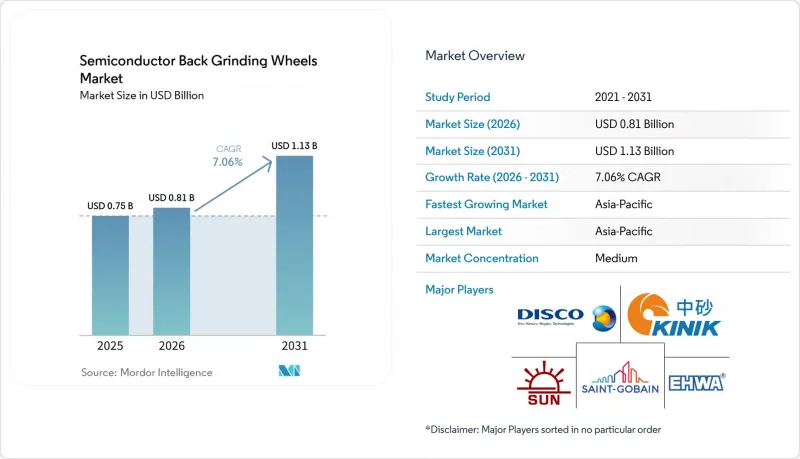
Global Semiconductor Back Grinding Wheels Market Trends and Insights
Advanced Packaging and Ultra-Thin Wafer Adoption
Advanced packaging has made wafer thinning a yield-critical process rather than a peripheral production step. In HBM3E and HBM4 flows, individual DRAM dies require thicknesses of 30 to 50 μm to meet package-height limits. Stacks with 20 or more layers will require thicknesses well below 30 μm, raising requirements for surface integrity and wheel performance. In February 2026, LINTEC introduced its Pattern Coating Before Lamination process and RAD-3400F/12 resin coater to reduce thickness variation caused by circuit-surface step heights. The process supports consistent performance from higher-grade wheels by reducing thickness variation at wafer entry, thereby reducing defects after back grinding. The semiconductor back-grinding wheels market also benefits as Outsourced Semiconductor Assembly and Test (OSAT) facilities adopt ultra-thin-wafer capabilities for fan-out wafer-level and panel-level packaging.
Expansion of 300 mm Wafer Manufacturing
The expansion of 300 mm manufacturing creates recurring demand for back-grinding consumables throughout a fab's operating life. SEMI expects global 300 mm front-end equipment spending to reach USD 142 billion in 2026, up 25% from 2025. SK Siltron began gradual operations at its 300 mm silicon wafer plant in the Gumi 3 Industrial Complex in July 2026, following a KRW 2.3 trillion investment (~USD 1.7 billion), and has secured customer orders supporting high-90% utilization. GlobalWafers opened its FAB300 facility in Novara, Italy, in October 2025, following a EUR 450 million investment (equivalent to USD 495 million). Migration from 5-inch and 6-inch wafers to 8-inch and 300 mm formats is also spreading across automotive microcontrollers, analog integrated circuits, and sensors, extending demand beyond advanced artificial intelligence devices.
Semiconductor Capital-Expenditure Cyclicality
Semiconductor capital spending is cyclical, and grinding-wheel sales can move with fab throughput, as wheels are variable consumables. Memory market volatility is particularly significant because memory fabs account for a large share of wafer-thinning output. SEMI reported sharp changes in NAND equipment spending. This variation can quickly affect fab utilization and reduce near-term demand for semiconductor back grinding wheels. Suppliers serving logic, memory, and power-device customers are better positioned to withstand a correction in any one of these device categories. Long qualification cycles also raise switching costs, as process changes can affect wafer yield and surface quality.
Other drivers and restraints analyzed in the detailed report include:
- SiC and GaN Power Semiconductor Scale-Up
- HBM, Chiplet, and 2.5D/3D Integration
- Diamond Grit, Cobalt, and Specialty Resin Supply Volatility
For complete list of drivers and restraints, kindly check the Table Of Contents.
Segment Analysis
Diamond grinding wheels held 63.45% of the semiconductor back grinding wheels market share in 2025 and are forecast to expand at an 8.06% CAGR through 2031. Their position reflects their ability to process silicon as well as harder, more brittle substrates such as SiC, GaN, and sapphire. Cubic Boron Nitride (CBN) and conventional abrasives cannot provide equivalent removal rates and damage control across the full range of materials entering high-volume production. A peer-reviewed 2024 study assessed five back-grinding wheel specifications across silicon, GaP, SiC, and sapphire. It found that bond modulus selection affected material removal and subsurface damage, with 122.07 GPa identified as the optimum bond modulus for SiC under the tested conditions. This technical requirement supports demand for qualified diamond products in the semiconductor back-grinding wheels market.
Vitrified-bond diamond wheels are gaining importance in ultra-precision fine-grinding stages because their porosity and self-sharpening behavior support consistent processing. Resin-bond diamond wheels remain important for finish-grinding steps where thermal stability requirements are less demanding. CBN wheels occupy a narrower role where contamination from cobalt-bonded diamond matrices is a concern. They may also serve selected compound-semiconductor structures where crystal sensitivity limits abrasive contact forces. Mixed-abrasive and advanced resin-bond formats are being developed for domestic SiC processing in China. These product developments indicate that the semiconductor back grinding wheels industry continues to require distinct wheel specifications for removal rate, thermal control, and surface integrity.
Complete Report Scope:
- By Abrasive Type
- Diamond Grinding Wheels
- CBN Grinding Wheels
- Others
- By Wafer and Substrate Material
- Silicon
- Silicon Carbide (SiC)
- Gallium Nitride (GaN)
- Sapphire
- Gallium Arsenide (GaAs)
- Others
- By Application
- Logic and Foundry Devices
- Memory Devices
- Power Semiconductors
- Compound Semiconductors and Optoelectronics
- Others
- By Geography
- Asia-Pacific
- China
- India
- Japan
- South Korea
- ASEAN Countries
- Rest of Asia-Pacific
- North America
- United States
- Canada
- Mexico
- Europe
- Germany
- United Kingdom
- France
- Italy
- NORDIC Countries
- Rest of Europe
- South America
- Brazil
- Argentina
- Rest of South America
- Middle East and Africa
- Saudi Arabia
- South Africa
- Rest of Middle East and Africa
- Asia-Pacific
Geography Analysis
Asia-Pacific held 44.76% of the semiconductor back grinding wheels market share in 2025 and is forecast to grow at an 8.42% CAGR through 2031. The region combines dense wafer fabrication, Outsourced Semiconductor Assembly and Test (OSAT), and grinding wheel manufacturing capacity across Japan, South Korea, Taiwan, and China. Japan remains a major center for wheel development and materials research. South Korean integrated device manufacturers operate high-capacity thinning lines for High Bandwidth Memory (HBM) and NAND production. Taiwan combines TSMC's advanced packaging activity with a broad OSAT network that requires 300 mm back grinding capacity. China is expanding mature-node semiconductor production while developing domestic grinding wheel capabilities.
North America recorded USD 10.9 billion in semiconductor equipment spending in 2025, supported by fab construction involving Intel, TSMC, Texas Instruments, and other manufacturers. GlobalWafers opened its USD 3.5 billion 300 mm silicon wafer facility in Sherman, Texas, in May 2025. These facilities create a multi-year demand base as production moves toward planned utilization. Europe recorded USD 2.9 billion in semiconductor equipment spending in 2025, a 41% decline from the prior year. European Commission grants totaling EUR 623 million (~USD 724.37 million) for facilities at GlobalFoundries in Dresden and X-FAB in Erfurt support a later recovery in regional wafer production.
South America, the Middle East, and Africa account for a smaller share of demand, as activity is concentrated in downstream electronics assembly rather than wafer fabrication. Saudi Arabia's Vision 2030 plans include developing a domestic semiconductor supply chain. India has a USD 15 billion semiconductor incentive program and approvals for ongoing fab construction. These programs establish conditions for future wheel demand later in the forecast period, though their near-term effect remains limited given the time required to build and qualify large-scale wafer fabrication facilities. The semiconductor back grinding wheels market will therefore remain centered on established production regions while newer locations develop supporting capacity.
- A.L.M.T. Corp.
- Asahi Diamond Industrial Co.,Ltd.
- DISCO CORPORATION
- EHWA DIAMOND
- KINIK COMPANY
- KURE GRINDING WHEEL
- Nanjing Sanchao Advanced Materials Co., Ltd
- NORITAKE CO., LIMITED
- Saesol Diamond
- Saint-Gobain
- Shinhan Diamond Ind. Co., Ltd.
- Suzhou Sail Science and Technology Co., Ltd.
- TOKYO SEIMITSU CO., LTD
- Tyrolit AG
- UKAM Industrial Superhard Tools
Additional Benefits:
- The market estimate (ME) sheet in Excel format
- 3 months of analyst support
TABLE OF CONTENTS
1 Introduction
- 1.1 Study Assumptions and Market Definition
- 1.2 Scope of the Study
2 Research Methodology
3 Executive Summary
4 Market Landscape
- 4.1 Market Overview
- 4.2 Market Drivers
- 4.2.1 Advanced Packaging and Ultra-Thin Wafer Adoption
- 4.2.2 Expansion of 300 mm Wafer Manufacturing
- 4.2.3 SiC and GaN Power Semiconductor Scale-Up
- 4.2.4 HBM, Chiplet and 2.5D/3D Integration
- 4.2.5 Mainstream Demand for High-Integrity Surface Finishing
- 4.2.6 In-Line Metrology and Closed-Loop Grinding Optimization
- 4.3 Market Restraints
- 4.3.1 Semiconductor Capital-Expenditure Cyclicality
- 4.3.2 Long Qualification Cycles and Yield-Cost Exposure
- 4.3.3 Diamond Grit, Cobalt and Specialty Resin Supply Volatility
- 4.3.4 Substitution by Laser, Plasma Dicing and CMP-Only Flows
- 4.4 Value and Supply-Chain Analysis
- 4.5 Porter's Five Forces Analysis
- 4.5.1 Threat of New Entrants
- 4.5.2 Bargaining Power of Suppliers
- 4.5.3 Bargaining Power of Buyers
- 4.5.4 Threat of Substitutes
- 4.5.5 Competitive Rivalry
5 Market Size and Growth Forecasts (Value)
- 5.1 By Abrasive Type
- 5.1.1 Diamond Grinding Wheels
- 5.1.2 CBN Grinding Wheels
- 5.1.3 Others
- 5.2 By Wafer and Substrate Material
- 5.2.1 Silicon
- 5.2.2 Silicon Carbide (SiC)
- 5.2.3 Gallium Nitride (GaN)
- 5.2.4 Sapphire
- 5.2.5 Gallium Arsenide (GaAs)
- 5.2.6 Others
- 5.3 By Application
- 5.3.1 Logic and Foundry Devices
- 5.3.2 Memory Devices
- 5.3.3 Power Semiconductors
- 5.3.4 Compound Semiconductors and Optoelectronics
- 5.3.5 Others
- 5.4 By Geography
- 5.4.1 Asia-Pacific
- 5.4.1.1 China
- 5.4.1.2 India
- 5.4.1.3 Japan
- 5.4.1.4 South Korea
- 5.4.1.5 ASEAN Countries
- 5.4.1.6 Rest of Asia-Pacific
- 5.4.2 North America
- 5.4.2.1 United States
- 5.4.2.2 Canada
- 5.4.2.3 Mexico
- 5.4.3 Europe
- 5.4.3.1 Germany
- 5.4.3.2 United Kingdom
- 5.4.3.3 France
- 5.4.3.4 Italy
- 5.4.3.5 NORDIC Countries
- 5.4.3.6 Rest of Europe
- 5.4.4 South America
- 5.4.4.1 Brazil
- 5.4.4.2 Argentina
- 5.4.4.3 Rest of South America
- 5.4.5 Middle East and Africa
- 5.4.5.1 Saudi Arabia
- 5.4.5.2 South Africa
- 5.4.5.3 Rest of Middle East and Africa
- 5.4.1 Asia-Pacific
6 Competitive Landscape
- 6.1 Market Concentration
- 6.2 Strategic Moves
- 6.3 Market Share (%)/Ranking Analysis
- 6.4 Company Profiles (includes Global Overview, Market Overview, Core Segments, Financials as available, Strategic Information, Products and Services, and Recent Developments)
- 6.4.1 A.L.M.T. Corp.
- 6.4.2 Asahi Diamond Industrial Co.,Ltd.
- 6.4.3 DISCO CORPORATION
- 6.4.4 EHWA DIAMOND
- 6.4.5 KINIK COMPANY
- 6.4.6 KURE GRINDING WHEEL
- 6.4.7 Nanjing Sanchao Advanced Materials Co., Ltd
- 6.4.8 NORITAKE CO., LIMITED
- 6.4.9 Saesol Diamond
- 6.4.10 Saint-Gobain
- 6.4.11 Shinhan Diamond Ind. Co., Ltd.
- 6.4.12 Suzhou Sail Science and Technology Co., Ltd.
- 6.4.13 TOKYO SEIMITSU CO., LTD
- 6.4.14 Tyrolit AG
- 6.4.15 UKAM Industrial Superhard Tools
7 Market Opportunities and Future Outlook
- 7.1 White-Space and Unmet-Need Assessment

