
PUBLISHER: Global Market Insights Inc. | PRODUCT CODE: 1844303

PUBLISHER: Global Market Insights Inc. | PRODUCT CODE: 1844303
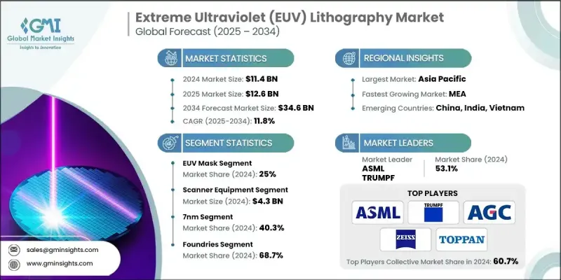
Extreme Ultraviolet (EUV) Lithography Market Opportunity, Growth Drivers, Industry Trend Analysis, and Forecast 2025 - 2034
The Global Extreme Ultraviolet Lithography Market was valued at USD 11.4 billion in 2024 and is estimated to grow at a CAGR of 11.8% to reach USD 34.6 billion by 2034.
This surge is attributed to EUV's critical role in advancing next-gen semiconductor manufacturing. As chipmakers increasingly transition to 5 nm and 3 nm process nodes, the demand for lithography systems capable of supporting finer geometries, higher integration density, and improved yields has grown substantially. The need for more efficient chips to power artificial intelligence, high-performance computing, and 5G applications is accelerating this shift. EUV lithography delivers the resolution and throughput required to manufacture complex integrated circuits with extreme precision. Additionally, rising capital expenditure by foundries and integrated device manufacturers (IDMs) across Asia-Pacific and North America, along with government-backed semiconductor initiatives, is fostering the adoption of EUV systems. Technological leadership from key suppliers and the industry's focus on scaling advanced logic and memory nodes are creating a sustained growth environment.
| Market Scope | |
|---|---|
| Start Year | 2024 |
| Forecast Year | 2025-2034 |
| Start Value | $11.4 billion |
| Forecast Value | $34.6 billion |
| CAGR | 11.8% |
In 2024, the light source segment generated USD 4.3 billion. This leadership is driven by the increasing demand for high-powered, stable EUV light sources, essential for high-volume chip production at cutting-edge nodes. Manufacturers continue to invest in improving the power and stability of these systems to enable precise wafer exposure and boost overall fab productivity. Enhancements in laser-produced plasma (LPP) systems have played a pivotal role in reducing system downtime and increasing throughput, making light source advancements a cornerstone of EUV technology expansion.
The mask inspection segment is anticipated to grow at a CAGR of 13% through 2034. This growth is propelled by the rising complexity of EUV photomasks, which demand highly sensitive and accurate inspection tools. As the industry evolves toward increasingly miniaturized and multi-patterned chip architectures, the need to detect even minute mask defects becomes vital to prevent yield loss. This trend is significantly driving investment in cutting-edge inspection technologies, establishing this segment as a critical growth contributor.
North America Extreme Ultraviolet (EUV) Lithography Market held a 26.7% share in 2024, representing a market value of USD 3 billion. The region's growth remains stable, underpinned by a robust semiconductor manufacturing ecosystem, rising demand for advanced chip architectures, and ongoing investments in AI and HPC infrastructure. Furthermore, the adoption of EUV tools for advanced logic nodes and innovative packaging solutions aligns with national priorities around technological leadership and supply chain security, reinforcing North America's position in the global market.
Key companies shaping the Global Extreme Ultraviolet (EUV) Lithography Market landscape include Carl Zeiss AG, NuFlare Technology Inc., Lasertec Corporation, Nikon Corporation, Photronics, Inc., ADVANTEST CORPORATION, Ushio Inc., SUSS MicroTec SE, Energetiq Technology, Inc., HOYA Corporation, TOPPAN Holdings Inc., AGC Inc., ASML, TRUMPF, and NTT Advanced Technology Corporation. To strengthen their market positioning, companies are investing in R&D to enhance light source performance, inspection accuracy, and mask handling technologies. Partnerships between OEMs and foundries are expanding to develop node-specific solutions, while supply chain diversification is being pursued to manage equipment lead times.
Table of Contents
Chapter 1 Methodology and Scope
- 1.1 Market scope and definition
- 1.2 Research design
- 1.2.1 Research approach
- 1.2.2 Data collection methods
- 1.3 Data mining sources
- 1.3.1 Global
- 1.3.2 Regional/Country
- 1.4 Base estimates and calculations
- 1.4.1 Base year calculation
- 1.4.2 Key trends for market estimation
- 1.5 Primary research and validation
- 1.5.1 Primary sources
- 1.6 Forecast model
- 1.7 Research assumptions and limitations
Chapter 2 Executive Summary
- 2.1 Industry 3600 synopsis
- 2.2 Key market trends
- 2.2.1 Component trends
- 2.2.2 Equipment type trends
- 2.2.3 Technology node trends
- 2.2.4 End Use trends
- 2.2.5 Regional
- 2.3 TAM Analysis, 2025-2034 (USD Million)
- 2.4 CXO perspectives: Strategic imperatives
- 2.4.1 Executive decision points
- 2.4.2 critical success factors
- 2.5 Future outlook and strategic recommendations
Chapter 3 Industry Insights
- 3.1 Industry ecosystem analysis
- 3.1.1 Supplier Landscape
- 3.1.2 Profit Margin
- 3.1.3 Cost structure
- 3.1.4 Value addition at each stage
- 3.1.5 Factor affecting the value chain
- 3.1.6 Disruptions
- 3.2 Industry impact forces
- 3.2.1 Growth drivers
- 3.2.1.1 Rising Demand for Sub-5nm and Sub-3nm Node Semiconductor Production
- 3.2.1.2 Surging AI, HPC, and 5G Chip Requirements
- 3.2.1.3 Government Semiconductor Incentive Programs (e.g., CHIPS and EU Chips Acts)
- 3.2.1.4 Monopolized Tool Supply and Technological Advancements by ASML
- 3.2.1.5 Expansion of Foundry and IDM Capex in Asia-Pacific and North America
- 3.2.2 Industry pitfalls and challenges
- 3.2.2.1 Extremely High Capital and Operational Costs
- 3.2.2.2 Complex Supply Chain and Limited Vendor Base (ASML Dependency)
- 3.2.3 Market opportunities
- 3.2.1 Growth drivers
- 3.3 Growth potential analysis
- 3.4 Regulatory landscape
- 3.4.1 North America
- 3.4.2 Europe
- 3.4.3 Asia Pacific
- 3.4.4 Latin America
- 3.4.5 Middle East & Africa
- 3.5 Porter’s analysis
- 3.6 PESTEL analysis
- 3.7 Technology and Innovation landscape
- 3.7.1 Current technological trends
- 3.7.2 Emerging technologies
- 3.8 Price trends
- 3.8.1 By region
- 3.8.2 By product
- 3.9 Pricing Strategies
- 3.10 Emerging Business Models
- 3.11 Compliance Requirements
- 3.12 Sustainability Measures
- 3.13 Consumer Sentiment Analysis
- 3.14 Patent and IP analysis
- 3.15 Geopolitical and trade dynamics
Chapter 4 Competitive Landscape, 2024
- 4.1 Introduction
- 4.2 Company market share analysis
- 4.2.1 By region
- 4.2.1.1 North America
- 4.2.1.2 Europe
- 4.2.1.3 Asia Pacific
- 4.2.1.4 Latin America
- 4.2.1.5 Middle East & Africa
- 4.2.2 Market Concentration Analysis
- 4.2.1 By region
- 4.3 Competitive benchmarking of key players
- 4.3.1 Financial performance comparison
- 4.3.1.1 Revenue
- 4.3.1.2 Profit margin
- 4.3.1.3 R&D
- 4.3.2 Product portfolio comparison
- 4.3.2.1 Product range breadth
- 4.3.2.2 Technology
- 4.3.2.3 Innovation
- 4.3.3 Geographic presence comparison
- 4.3.3.1 Global footprint analysis
- 4.3.3.2 Service network coverage
- 4.3.3.3 Market penetration by region
- 4.3.4 Competitive positioning matrix
- 4.3.4.1 Leaders
- 4.3.4.2 Challengers
- 4.3.4.3 Followers
- 4.3.4.4 Niche players
- 4.3.5 Strategic outlook matrix
- 4.3.1 Financial performance comparison
- 4.4 Key developments, 2021-2024
- 4.4.1 Mergers and acquisitions
- 4.4.2 Partnerships and collaborations
- 4.4.3 Technological advancements
- 4.4.4 Expansion and investment strategies
- 4.4.5 Sustainability initiatives
- 4.4.6 Digital transformation initiatives
- 4.5 Emerging/ startup competitors landscape
Chapter 5 Market Estimates and Forecast, By Component, 2021 - 2034 (USD Million)
- 5.1 Key trends
- 5.2 Light Source
- 5.3 EUV Mask
- 5.4 EUV Optics
- 5.5 Metrology Equipment
- 5.6 Others
Chapter 6 Market Estimates and Forecast, By Equipment Type, 2021 - 2034 (USD Million)
- 6.1 Key trends
- 6.2 Scanner Equipment
- 6.3 Mask Inspection Equipment
- 6.4 Pellicles and Reticle Handling
- 6.5 Track Systems (Coater/Developer)
Chapter 7 Market Estimates and Forecast, By Technology Node, 2021 - 2034 (USD Million)
- 7.1 Key trends
- 7.2 7nm
- 7.3 5nm
- 7.4 3nm
Chapter 8 Market Estimates and Forecast, By End Use, 2021 - 2034 (USD Million)
- 8.1 Key trends
- 8.2 Integrated Device Manufacturers
- 8.3 Foundries
Chapter 9 Market Estimates and Forecast, By Region, 2021 - 2034 (USD Million)
- 9.1 Key trends
- 9.2 North America
- 9.2.1 U.S.
- 9.2.2 Canada
- 9.3 Europe
- 9.3.1 Germany
- 9.3.2 UK
- 9.3.3 France
- 9.3.4 Spain
- 9.3.5 Italy
- 9.3.6 Netherlands
- 9.4 Asia Pacific
- 9.4.1 China
- 9.4.2 India
- 9.4.3 Japan
- 9.4.4 Australia
- 9.4.5 South Korea
- 9.5 Latin America
- 9.5.1 Brazil
- 9.5.2 Mexico
- 9.5.3 Argentina
- 9.6 Middle East and Africa
- 9.6.1 Saudi Arabia
- 9.6.2 South Africa
- 9.6.3 UAE
Chapter 10 Company Profiles
- 10.1 ADVANTEST CORPORATION
- 10.2 AGC Inc.
- 10.3 ASML
- 10.4 Carl Zeiss AG
- 10.5 Energetiq Technology, Inc.
- 10.6 HOYA Corporation
- 10.7 Lasertec Corporation
- 10.8 NTT Advanced Technology Corporation
- 10.9 Nikon Corporation
- 10.10 NuFlare Technology Inc.
- 10.11 Photronics, Inc.
- 10.12 TOPPAN Holdings Inc.
- 10.13 TRUMPF
- 10.14 SUSS MicroTec SE
- 10.15 Ushio Inc.

