
PUBLISHER: Mordor Intelligence | PRODUCT CODE: 1693685

PUBLISHER: Mordor Intelligence | PRODUCT CODE: 1693685
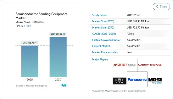
Semiconductor Bonding Equipment - Market Share Analysis, Industry Trends & Statistics, Growth Forecasts (2025 - 2030)
The Semiconductor Bonding Equipment Market size is estimated at USD 568.96 million in 2025, and is expected to reach USD 722.70 million by 2030, at a CAGR of 4.9% during the forecast period (2025-2030).
Semiconductor bonding equipment finds application owing to the rising demand for semiconductor chips with higher efficiency, processing power, and smaller footprint, thereby driving the demand for the market during the forecast period.
Key Highlights
- As the impact of digitalization has increased, semiconductor markets have boomed. Notably, this has further resulted in government programs to support the 5G deployment. For instance, the European Commission recognized the importance of the 5G network early and established a public-private partnership to develop and research 5G technology.
- With chip demand set to surge over the coming decade, the global semiconductor industry is expected to become a trillion-dollar industry by 2030. This growth is favored by companies and countries funneling vast sums of money into semiconductor manufacturing, materials, and research to guarantee a constant supply of chips and know-how to support growth across a broad swath of increasingly data-centric industries.
- The semiconductor industry, which makes crucial technological components, has been hitting the headlines due to a rampant demand increase. A recent Wall Street Journal report shows that semiconductors rank as the world's fourth-largest traded product (imports and exports, counted), after crude oil, refined oil, and cars. This is because semiconductors are critical for high-computing applications in various industries, including electronics and manufacturing industries, agriculture, healthcare, infrastructure, entertainment, transportation, telecommunications, military systems, energy management, and space, to name just a few.
- Several methods might be used when a product needs the bonding of two dies or wafers. Not only does the type of bonding method itself have to be selected, but it must also be decided whether the items being bonded will be in wafer or die form. The selected bonding process is the primary driver for the cost of ownership of bonding. For a given process, the three most important factors are the cost of the upstream process needed for bonding, the cycle time of the bonding process, and the yield of the bonding process.
- With the global outbreak of the pandemic and restrictive measures taken to control the spread of COVID-19, the global supply chain of the semiconductor bonding equipment industry was significantly disrupted, impacting the production capabilities of various companies. Although the number of COVID-19-infected patients decreased considerably, salient issues with materials supply and demand for these components still need to be addressed, challenging the market's growth.
Semiconductor Bonding Equipment Market Trends
Power IC and Power Discrete Application Segment Holds Significant Market Share
- Power semiconductor devices facilitate efficient power management, conversion, and control across various applications. The increasing focus on energy conservation and power consumption is increasing the significance of power semiconductor devices. The market is supported by reduced losses, enhanced controllability, greater durability, and reliable performance in standard and fault conditions. As the demand for power semiconductors continues to rise, there is also an expected increase in the market for power ICs and bonding technology.
- The segment's growth is driven by the rapid digitization of industries and the increasing number of connected devices. These devices necessitate efficient power management and high-performance power semiconductor devices. By utilizing these devices, optimal power conversion is achieved, energy losses are reduced, and the overall energy efficiency of electronic systems is enhanced.
- The segment is experiencing growth due to the rising demand for high-energy and power-efficient devices. This demand is further fueled by the prevalence of wireless and portable electronic products, the automotive industry's shift toward electrification, and the increased use of these devices.
- The industry has a rising inclination toward power modules and integrated solutions. Manufacturers of power semiconductors are creating compact, highly integrated modules that merge various power components like switches, diodes, and drivers to streamline system design, lower component quantity, and improve overall system efficiency. Power semiconductor firms stand to gain by understanding the obstacles and market trends early in the product design process to remain competitive. The increasing investments by vendors to boost power semiconductor production are anticipated to affect the market's expansion.
- A significant development in power IC and discrete components enhances power management efficiency. Recent advancements in system architectures have led to more efficient AC-DC power adapters with reduced size and component numbers. Introducing new Power-over-Ethernet (PoE) standards has enabled higher power transfer capabilities, facilitating the creation of innovative device categories like connected lighting. The growing emphasis on minimizing electricity consumption by electronics manufacturers and the increasing demand from consumer electronics are the primary drivers behind the necessity for Power ICs. These factors could potentially boost the demand for bonding equipment.
- There is a significant rise in smartphone transmission speeds, necessitating battery modules to accommodate the processing requirements. Power adapters are now incorporating discrete semiconductors, leading to an anticipated surge in demand driven by the increasing sales of battery-powered devices. The growth of IoT applications is projected to propel the demand for discrete semiconductors further.
- For example, according to Ericsson, global cellular IoT connections reached 1.9 billion in 2022 and are estimated to reach 5.5 billion by 2027. The increasing penetration of smartphones with the evolution of 5G is expected to drive the market's growth.
- Similarly, the market's growth is expected to be positively influenced by the significant technological advancements in IoT applications, which aim to provide technologically enhanced linked devices to consumers worldwide. The expansion of IoT applications has increased the prevalence of smart devices and small semiconductors, consequently driving the demand for advanced semiconductor bonding equipment.
- Ericsson stated that the number of connected devices globally will nearly double from 2022 to 2028, primarily due to the rise in short-range IoT devices. It is expected that there will be approximately 28.72 billion such devices by 2028. With the growing demand for these IoT-connected devices, the demand for power ICs is expected to rise, thereby enhancing the growth of the bonding equipment market.
Asia-Pacific is Expected to be the Fastest Growing Market
- The semiconductor industry has emerged as a critical driver of economic growth in Asia. Its rapid expansion and technological advancements have become an important component of the global supply chain.
- Asia-Pacific holds a major share of semiconductor foundries globally, with the region having the presence of prominent companies like Samsung Electronics, TSMC, etc. South Korea, Taiwan, Japan, and China have significant market shares in the region. Taiwan holds a prominent share of the foundries in the world and is a vital region in the semiconductor value chain. The increasing investments in the expansion of semiconductor manufacturing capacities in the region are expected to aid the market's growth significantly.
- In September 2023, China launched a USD 40 billion fund to boost the semiconductor industry. China plans to establish a state-backed investment fund to narrow the gap with global rivals, especially the United States. This initiative is poised to evolve as the most significant of the trio of funds managed by the China Integrated Circuit Industry Investment Fund, generally known as the Big Fund. President Xi Jinping of China stressed the critical importance of achieving semiconductor self-sufficiency, primarily in response to export control measures imposed by the United States. The latest fund obtained approval from Chinese authorities, with the finance ministry committing CNY 60 billion (USD 8.30 billion).
- Based on its expanding domestic chip demand, China is estimated to overtake the United States as the world's top powerhouse in the semiconductor industry. By 2030, the semiconductor market is expected to double in size to reach more than USD 1 trillion, with China contributing over 60% of that increase, according to the Semiconductor Industry Association. Such exponential growth is anticipated to increase demand for semiconductor bonding equipment.
- The new semiconductor fab would fabricate chips for applications like display drivers, power management IC, microcontrollers, and high-performance computing logic, addressing the growing demand in markets like computing and data storage, automotive, wireless communication, and artificial intelligence. This fab claims to have a manufacturing capacity of up to 50,000 wafers per month, and the first chip will come out of the facility before the end of 2026.
Semiconductor Bonding Equipment Market Overview
The semiconductor bonding equipment market is highly fragmented, with major players like EV Group, ASMPT Semiconductor Solutions, MRSI Systems (Myronic AB), WestBond Inc., and Panasonic Holding Corporation. Market players participate in partnerships and acquisitions to gain sustainable competitive advantage and enhance their product offerings.
- November 2023 - The EV Group (EVG) announced the completion of construction works for the next phase of the expansion of EVG corporate headquarters. The "Manufacturing V" facility serves as EVG's manufacturing department for equipment components and offers a significant expansion of production floor and warehouse space. The opening of the Manufacturing V facility marks the latest expansion phase and investment of EVG, which continues to benefit from the continuing high demand for EVG's hybrid bonding solutions and other process solutions, as well as process development services, to support the fast-growing advanced packaging market and 3D / heterogeneous integration market.
- September 2023 - MRSI Systems (Mycronic AB) announced the launch of the new variant of the well-established MRSI-7001 platform, the MRSI 7001HF. The 7001HF features a heated bond head capable of applying up to 500N forces during bonding. The heated bond head also provides heating from the top at a temperature of 400°C. This makes the 7001HF the perfect tool for high-force die bonders for applications such as power semiconductor sintering for IC packaging or thermocompression bonders for IC packaging.
Additional Benefits:
- The market estimate (ME) sheet in Excel format
- 3 months of analyst support
TABLE OF CONTENTS
1 INTRODUCTION
- 1.1 Study Assumptions and Market Definition
- 1.2 Scope of the Study
2 RESEARCH METHODOLOGY
3 EXECUTIVE SUMMARY
4 MARKET INSIGHTS
- 4.1 Market Overview
- 4.2 Market Attractiveness - Porter's Five Forces Analysis
- 4.2.1 Bargaining Power of Suppliers
- 4.2.2 Bargaining Power of Buyers
- 4.2.3 Threat of New Entrants
- 4.2.4 Threat of Substitutes
- 4.2.5 Intensity of Competitive Rivalry
- 4.3 Industry Value Chain/Supply Chain Analysis
- 4.4 Impact of COVID-19 on the Market
5 Market Dynamics
- 5.1 Market Driver
- 5.1.1 Increasing Investment by Semiconductor Manufacturers to Expand their Manufacturing Capacity
- 5.1.2 Rising Demand for Semiconductor Chips across Various Application
- 5.2 Market Restraints
- 5.2.1 High Cost of Ownership
- 5.2.2 Increased Complexity Owing to Miniaturization of Circuits
6 MARKET SEGMENTATION
- 6.1 By Type
- 6.1.1 Permanent Bonding Equipment
- 6.1.2 Temporary Bonding Equipment
- 6.1.3 Hybrid Bonding Equipment
- 6.2 By Application
- 6.2.1 Advanced Packaging
- 6.2.2 Power IC and Power Discrete
- 6.2.3 Photonic Devices
- 6.2.4 MEMS Sensors and Actuators
- 6.2.5 Engineered Substrates
- 6.2.6 RF Devices
- 6.2.7 CMOS Image Sensors (CIS)
- 6.3 By Geography
- 6.3.1 North America
- 6.3.2 Europe
- 6.3.3 Asia
- 6.3.4 Australia and New Zealand
- 6.3.5 Latin America
- 6.3.6 Middle East and Africa
7 COMPETITIVE LANDSCAPE
- 7.1 Company Profiles
- 7.1.1 EV Group
- 7.1.2 ASMPT Semiconductor Solutions
- 7.1.3 MRSI Systems. (Myronic AB)
- 7.1.4 WestBond Inc.
- 7.1.5 Panasonic Holding Corporation
- 7.1.6 Palomar Technologies
- 7.1.7 Dr. Tresky AG
- 7.1.8 BE Semiconductor Industries NV
- 7.1.9 Fasford Technology Co.Ltd (Fuji Group)
- 7.1.10 Kulicke and Soffa Industries Inc.
- 7.1.11 DIAS Automation (HK) Ltd
- 7.1.12 Shibaura Mechatronics Corporation
- 7.1.13 SUSS MicroTec SE
- 7.1.14 Tokyo Electron Limited
8 INVESTMENT ANALYSIS
9 FUTURE OF THE MARKET

