
PUBLISHER: Mordor Intelligence | PRODUCT CODE: 1851112

PUBLISHER: Mordor Intelligence | PRODUCT CODE: 1851112
Semiconductor Equipment - Market Share Analysis, Industry Trends & Statistics, Growth Forecasts (2025 - 2030)
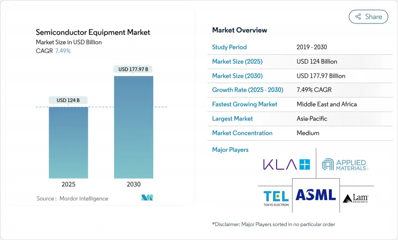
The semiconductor equipment market size was valued at USD 124.00 billion in 2025 and is forecast to reach USD 177.97 billion by 2030, at a 7.49% CAGR.
Robust fab construction, record equipment backlogs, and a wave of government incentives underpin this trajectory. Foundries are accelerating capacity at 2 nm and below, while Outsourced Semiconductor Assembly and Test (OSAT) players scale advanced-package lines to serve artificial-intelligence (AI) demand. Geopolitical efforts to achieve technological sovereignty are shaping capital-spending patterns, forcing tool vendors to juggle export controls in China with subsidy-fuelled opportunities in North America, Europe, and the Middle East. Equipment makers that bundle process breadth, software analytics, and service coverage are securing multi-year purchase commitments from the sector's largest investors.
Global Semiconductor Equipment Market Trends and Insights
Surging demand for advanced consumer electronics and smartphones
Smartphones, wearables, and mixed-reality devices keep adding logic, memory, and analog content that must be built at ever-smaller nodes, pushing foundries to accelerate capacity on 28 nm-7 nm lines. Advanced packaging that miniaturizes high-bandwidth functions without raising power budgets drove a sizable share of early-2025 revenue, triggering an upgrade wave in bumping, test, and lithography equipment. Heterogeneous-integration lines stacking chiplets vertically are expanding at double-digit rates, lifting shipments of flip-chip bonders and wafer-level inspection tools. Tool makers offering modular deposition chambers with rapid recipe switching are winning orders as consumer-product cycles tighten. Strong handset refresh rates across India and Southeast Asia keep mature-node tools running near full utilization, proving that resilient billings are achievable even during premium-device launches.
Rapid AI-, IoT- and edge-device node investments
Data-center operators seek chips that offer higher TOPS-per-watt, boosting procurement of extreme ultraviolet (EUV) scanners and atomic-layer deposition modules used at 3 nm and below. AI accelerator start-ups in the United States and Europe are signing capacity reservation agreements that tie multi-year HBM purchases to guaranteed access to leading-edge lithography, shifting demand risk from chip designers to equipment makers. Edge AI devices for factory automation and smart-city deployments accelerate 16 nm-12 nm demand, spurring fresh orders for 300 mm etch systems tailored to embedded non-volatile memory. Tool suppliers deploy AI in situ process-monitoring algorithms, shortening recipe-development cycles and improving chamber uptime. The self-reinforcing loop between AI workload growth and smarter tools bolsters the semiconductor equipment market well past 2030.
Extremely high CAPEX and long pay-back cycles
A single advanced-logic fab now costs well above USD 20 billion, making the customer base for leading-edge tools increasingly concentrated. Lengthy depreciation periods stretch procurement scrutiny, compelling toolmakers to demonstrate multi-node extendibility before purchase orders are released. Vendors respond with upgrade-ready platforms, modular vacuum geometries, and subscription-based process-control software that spreads cost over a tool's life span. Some IDMs delay capacity expansions, which defers installations and shifts revenue recognition to late project phases. Nevertheless, the relentless need for performance-per-watt keeps road maps intact, limiting the overall drag on the semiconductor equipment market.
Other drivers and restraints analyzed in the detailed report include:
- Government subsidy waves are boosting the tool CAPEX
- Transition to GAA and High-NA EUV necessitates new toolsets
- Specialty-material supply bottlenecks are delaying tool shipments
For complete list of drivers and restraints, kindly check the Table Of Contents.
Segment Analysis
Front-end wafer-processing instruments captured 83.7% of the semiconductor equipment market share in 2024, underscoring the central role of lithography, etch, and deposition in yield improvement. Within this segment, High-NA EUV scanners post a 21.1% CAGR to 2030 because they are indispensable for patterning 2 nm logic and 3-D DRAM structures; multi-system orders from fabs in Taiwan and New York already total several billion USD.
Backend complexity fuels innovations such as thermo-compression bonders with sub-2 µm alignment accuracy and fan-out wafer-level packaging that leverages front-end lithographic precision. Vendors that combine lithography optics, placement robotics, and high-frequency test modules into unified platforms are capturing a growing share of advanced-package budgets, extending lithography-grade investments further down the supply chain.
Foundries accounted for 52.2% of semiconductor equipment market revenue in 2024 as fabless chip firms concentrate orders on TSMC, Samsung Foundry, and GlobalFoundries. Mega-projects in Arizona, Dresden, and Kaohsiung each feature clusters of EUV scanners, multi-chamber etch stacks, and atomic-layer deposition tools configured for rapid recipe swaps, reflecting the foundry model's need to host diverse customer process flows. Strict uptime commitments drive bundled service contracts that now equal 25-30% of tool acquisition value, creating annuity streams for equipment suppliers.
OSAT houses emerge as the fastest-growing customer category at a 12.2% CAGR, propelled by 2.5-D and 3-D package architectures required for AI accelerators and automotive domain controllers. New capex lines include laser-drilling for through-silicon vias, high-density flip-chip bonders, and molded-underfill dispense systems. Integrated device manufacturers (IDMs) retain a sizeable but declining share as they pursue fab-lite strategies that outsource leading-edge logic while investing selectively in power, analog, and sensor lines.
Semiconductor Equipment Market is Segmented by Equipment Type (Front-End Equipment, and Back-End Equipment), Supply Chain Participant (IDM, Foundry, and OSAT), Wafer Size (300 Mm, 200 Mm, and <=150 Mm), Fab Technology Node (>=28 Nm, 16/14 Nm, and More), End-User Industry (Computing and Data-Center, Communications (5G, RF), and More), and Geography (North America, South America, Europe, Asia-Pacific, and Middle East and Africa).
Geography Analysis
Asia-Pacific retained 72.2% semiconductor equipment market share in 2024, powered by dense ecosystems in Taiwan, South Korea, and mainland China; Taiwan's foundry cluster alone ran above 90% utilization, sustaining EUV and metrology orders. South Korea intensified spending on 1-beta DRAM and gate-all-around logic, while China's drive for self-reliance lifted domestic etcher and deposition installations even under export-control pressure.
North America's renaissance stems from CHIPS Act grants; Albany NanoTech took delivery of the world's first High-NA EUV tool, creating a cornerstone for a domestic lithography ecosystem. Simultaneous investments by TSMC and Intel in Arizona form a corridor stretching from equipment assembly in Oregon to materials supply in Texas, re-balancing regional demand.
Europe sharpened its specialty-technology focus-automotive power devices, RF front-ends, and advanced sensors-using the European Chips Act to target a doubling of regional capacity by 2030; Saxony's dual 300 mm lines already combine logic, analog, and power processing.
The Middle East and Africa logged the fastest growth at 9.9% CAGR, fuelled by Saudi Arabia's USD 9 billion fab plan and UAE feasibility studies, which require turnkey tool-support contracts spanning training, refurbishment, and logistics. South America remains niche; Brazil is investing selectively in automotive and industrial chips that rely on mature-node 200 mm tools.
- Applied Materials Inc.
- ASML Holding NV
- Tokyo Electron Ltd.
- Lam Research Corp.
- KLA Corp.
- Screen Holdings Co. Ltd.
- Teradyne Inc.
- Hitachi High-Tech Corp.
- Veeco Instruments Inc.
- ASM International NV
- Canon Inc.
- Nikon Corp.
- Onto Innovation Inc.
- Nova Ltd.
- Advantest Corp.
- Hanmi Semiconductor Co. Ltd.
- Disco Corp.
- BESI (BE Semiconductor Industries)
- Kulicke & Soffa Industries Inc.
- FormFactor Inc.
- Plasma-Therm LLC
- SUSS MicroTec SE
- Kokusai Electric Corp.
- AMEC (Advanced Micro-Fabrication Equipment Inc.)
- Naura Technology Group Co. Ltd.
Additional Benefits:
- The market estimate (ME) sheet in Excel format
- 3 months of analyst support
TABLE OF CONTENTS
1 INTRODUCTION
- 1.1 Study Assumptions and Market Definition
- 1.2 Scope of the Study
2 RESEARCH METHODOLOGY
3 EXECUTIVE SUMMARY
4 MARKET LANDSCAPE
- 4.1 Market Overview
- 4.2 Market Drivers
- 4.2.1 Surging demand for advanced consumer electronics and smartphones
- 4.2.2 Rapid AI-, IoT- and edge-device node investments
- 4.2.3 Government subsidy waves (CHIPS, EU Chips Act, etc.) boosting tool CAPEX
- 4.2.4 Transition to GAA and High-NA EUV necessitating new toolsets
- 4.2.5 Sustainability mandates driving "green fab" retrofit tools
- 4.2.6 3D heterogeneous-integration packaging demand spike
- 4.3 Market Restraints
- 4.3.1 Extremely high CAPEX and long pay-back cycles
- 4.3.2 Specialty-material supply bottlenecks delaying tool shipments
- 4.3.3 Export-control restrictions on China-bound tools
- 4.3.4 Acute shortage of skilled field-service engineers
- 4.4 Value Chain Analysis
- 4.5 Regulatory Landscape
- 4.6 Technological Outlook
- 4.7 Porter's Five Forces Analysis
- 4.7.1 Bargaining Power of Suppliers
- 4.7.2 Bargaining Power of Buyers
- 4.7.3 Threat of New Entrants
- 4.7.4 Threat of Substitutes
- 4.7.5 Intensity of Competitive Rivalry
- 4.8 Impact of Macroeconomic Factors
5 MARKET SIZE AND GROWTH FORECASTS (VALUE)
- 5.1 By Equipment Type
- 5.1.1 Front-end Equipment
- 5.1.1.1 Lithography Equipment
- 5.1.1.2 Etch Equipment
- 5.1.1.3 Deposition Equipment
- 5.1.1.4 Metrology / Inspection Equipment
- 5.1.1.5 Cleaning Equipment
- 5.1.1.6 Photoresist Processing Equipment
- 5.1.1.7 Other Front-end Types
- 5.1.2 Back-end Equipment
- 5.1.2.1 Test Equipment
- 5.1.2.2 Assembly and Packaging Equipment
- 5.1.1 Front-end Equipment
- 5.2 By Supply-Chain Participant
- 5.2.1 IDM
- 5.2.2 Foundry
- 5.2.3 OSAT
- 5.3 By Wafer Size
- 5.3.1 300 mm
- 5.3.2 200 mm
- 5.3.3 <=150 mm
- 5.4 By Fab Technology Node
- 5.4.1 >=28 nm
- 5.4.2 16/14 nm
- 5.4.3 10/7 nm
- 5.4.4 5 nm and below
- 5.5 By End-user Industry
- 5.5.1 Computing and Data-Center
- 5.5.2 Communications (5G, RF)
- 5.5.3 Automotive and Mobility
- 5.5.4 Consumer Electronics
- 5.5.5 Industrial and Others
- 5.6 By Geography
- 5.6.1 North America
- 5.6.1.1 United States
- 5.6.1.2 Canada
- 5.6.1.3 Mexico
- 5.6.2 South America
- 5.6.2.1 Brazil
- 5.6.2.2 Argentina
- 5.6.2.3 Rest of South America
- 5.6.3 Europe
- 5.6.3.1 Germany
- 5.6.3.2 United Kingdom
- 5.6.3.3 France
- 5.6.3.4 Italy
- 5.6.3.5 Spain
- 5.6.3.6 Rest of Europe
- 5.6.4 Asia-Pacific
- 5.6.4.1 China
- 5.6.4.2 Japan
- 5.6.4.3 South Korea
- 5.6.4.4 India
- 5.6.4.5 Rest of Asia-Pacific
- 5.6.5 Middle East and Africa
- 5.6.5.1 Middle East
- 5.6.5.1.1 Saudi Arabia
- 5.6.5.1.2 United Arab Emirates
- 5.6.5.1.3 Turkey
- 5.6.5.1.4 Rest of Middle East
- 5.6.5.2 Africa
- 5.6.5.2.1 South Africa
- 5.6.5.2.2 Nigeria
- 5.6.5.2.3 Egypt
- 5.6.5.2.4 Rest of Africa
- 5.6.1 North America
6 COMPETITIVE LANDSCAPE
- 6.1 Market Concentration
- 6.2 Strategic Moves
- 6.3 Market Share Analysis
- 6.4 Company Profiles (includes Global-level Overview, Market-level Overview, Core Segments, Financials as available, Strategic Information, Market Rank/Share, Products and Services, Recent Developments)
- 6.4.1 Applied Materials Inc.
- 6.4.2 ASML Holding NV
- 6.4.3 Tokyo Electron Ltd.
- 6.4.4 Lam Research Corp.
- 6.4.5 KLA Corp.
- 6.4.6 Screen Holdings Co. Ltd.
- 6.4.7 Teradyne Inc.
- 6.4.8 Hitachi High-Tech Corp.
- 6.4.9 Veeco Instruments Inc.
- 6.4.10 ASM International NV
- 6.4.11 Canon Inc.
- 6.4.12 Nikon Corp.
- 6.4.13 Onto Innovation Inc.
- 6.4.14 Nova Ltd.
- 6.4.15 Advantest Corp.
- 6.4.16 Hanmi Semiconductor Co. Ltd.
- 6.4.17 Disco Corp.
- 6.4.18 BESI (BE Semiconductor Industries)
- 6.4.19 Kulicke & Soffa Industries Inc.
- 6.4.20 FormFactor Inc.
- 6.4.21 Plasma-Therm LLC
- 6.4.22 SUSS MicroTec SE
- 6.4.23 Kokusai Electric Corp.
- 6.4.24 AMEC (Advanced Micro-Fabrication Equipment Inc.)
- 6.4.25 Naura Technology Group Co. Ltd.
7 MARKET OPPORTUNITIES AND FUTURE OUTLOOK
- 7.1 White-space and Unmet-Need Assessment

