
PUBLISHER: Mordor Intelligence | PRODUCT CODE: 1939642

PUBLISHER: Mordor Intelligence | PRODUCT CODE: 1939642
Dielectric Etchers - Market Share Analysis, Industry Trends & Statistics, Growth Forecasts (2026 - 2031)
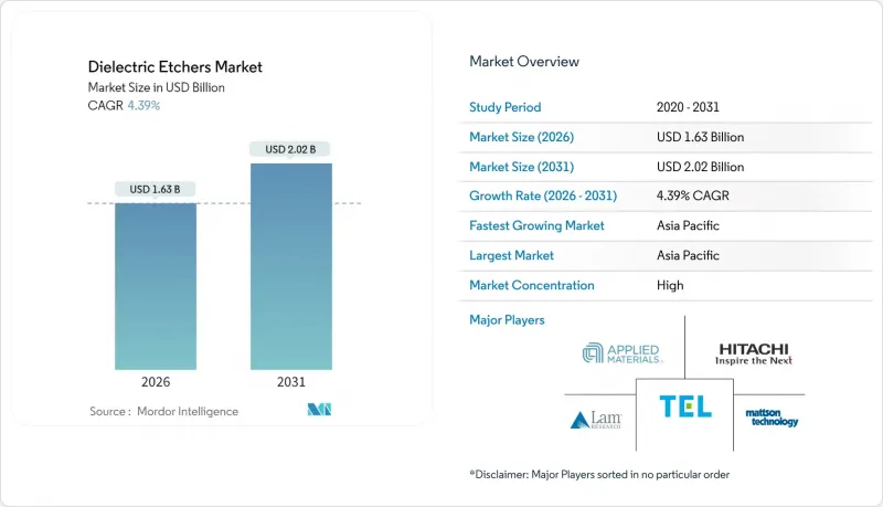
The dielectric etchers market size in 2026 is estimated at USD 1.63 billion, growing from 2025 value of USD 1.56 billion with 2031 projections showing USD 2.02 billion, growing at 4.39% CAGR over 2026-2031.
Rising atomic-layer precision needs at sub-7 nm, escalating 3D NAND layer counts and low-k dielectric adoption in advanced packaging keep capital spending elevated even when device demand cools. Foundries continue to drive the dielectric etchers market as gate-all-around (GAA) logic and heterogeneous integration shorten equipment replacement cycles. Regionally, Asia Pacific dominates installations, but CHIPS Act-funded fabs in North America and EU Chips initiatives are reshaping procurement geography. Vendors with multi-material process know-how and domestic supply chains are best positioned to capture the current wave of re-tooling, while precision enhancements such as atomic-layer etching (ALE) and cryogenic plasma modules create new differentiation avenues.
Global Dielectric Etchers Market Trends and Insights
Proliferation of Sub-7 nm Logic Nodes
Sub-7 nm production raises mask counts and shrinks process windows, pushing etch step totals 40-60% higher than 10 nm flows. GAA transistors require sacrificial SiGe removal without scarring high-k layers, forcing fabs to swap legacy chambers for ALE-ready tools. TSMC's USD 38-42 billion 2025 capex focuses on 2 nm pilot lines, locking in multi-year orders for high-selectivity dielectric modules. Because node migrations now coincide with packaging overhauls, tool refreshes happen on a three-year rather than five-year cadence, anchoring steady revenue for the dielectric etchers market. Equipment makers that can co-develop chemistries with customers enjoy preferred-supplier status, reinforcing market entry barriers.
3D NAND Layer-Count Escalation
Etching 64 µm-deep channel holes through above 400-layer stacks demands aspect-ratio control near 100:1, pressuring plasma uniformity and by-product evacuation. Cryogenic etch launched by Tokyo Electron in 2025 mitigates bowing and twisting, answering Lam Research's hold in memory etch. Each 32-layer leap forces chamber redesigns, driving an 18-24 month replacement cycle at Samsung and other NAND leaders. The dielectric etchers market therefore benefits from memory spending even during logic lulls, buffering revenue volatility.
High Capital Intensity of Etch Tools
State-of-the-art dielectric chambers cost USD 5-8 million, and ALE clusters can top USD 12-15 million installed. Board-level approvals and extended leasing reviews delay installs 6-12 months, especially at smaller IDMs and specialty fabs. Vendors respond with modular platforms that share RF, vacuum, and wafer-handling subsystems to spread expenses across process nodes, yet budget ceilings still trim the near-term dielectric etchers market expansion rate by 70 basis points.
Other drivers and restraints analyzed in the detailed report include:
- Low-k Dielectric Adoption in Advanced Packaging
- Rising 5G/AI Chip Volumes
- Semiconductor CAPEX Cyclicality
For complete list of drivers and restraints, kindly check the Table Of Contents.
Segment Analysis
Silicon dioxide retained 38.10% dielectric etchers market share in 2025, anchoring mature logic and DRAM flows where cost trumps performance. The dielectric etchers market size for low-k materials is projected to balloon alongside a 468.12% CAGR, reflecting AI accelerators' need for minimal capacitance substrates.
Low-k adoption compels plasma chemistries that avoid carbon depletion and copper corrosion, spurring multi-frequency RF innovations that established vendors alone can commercialize at scale. Simultaneously, silicon nitride and emerging glass dielectrics hold niche roles for barrier and panel-level packaging, demanding etch selectivity previously unseen. This broadening palette obliges toolmakers to bundle in situ endpoint metrology and multi-pressure chambers, reinforcing switching costs and sustaining revenue diversity across the dielectric etchers market.
Reactive-ion etching commanded 42.26% of the dielectric etchers market in 2025 and remains the workhorse for cost-sensitive layers. However, ALE's 5.02% annual growth underscores its inevitability for GAA, 3D NAND and quantum circuits.
Manufacturers weigh throughput penalties against yield gains; pilot data show defect-density cuts of 35-45% when ALE replaces multi-step RIE on fin sidewalls. Tokyo Electron's cryogenic RIE hybrid blurs boundaries, letting fabs phase-in ALE tactically while protecting cycle-time budgets. Such hybridization keeps the dielectric etchers market fragmented, enabling mid-tier suppliers to carve out niches in microwave plasma or UV-assisted processes.
The Global Dielectric Etchers Market Report is Segmented by Dielectric Material (Silicon Dioxide, Silicon Nitride, and More), Technology (Reactive-Ion Etching, Inductively-Coupled Plasma, and More), Wafer Size (less Than 150mm, 200mm, 300mm, and More), End User (Pure-Play Foundries, Idms, MEMS and Sensor Fabs, and R&D and Pilot Lines), and Geography. The Market Forecasts are Provided in Terms of Value (USD).
Geography Analysis
Asia Pacific accounted for 64.51% of dielectric etchers market size in 2025 on the strength of Korean memory and Taiwanese logic clusters. China alone delivered 42% of Lam Research's revenue, yet export-control headwinds compel dual-sourcing and localized toolmaking. Governments across Japan, India and Singapore fund backend ecosystems, widening regional tool demand beyond legacy hubs.
North America's CHIPS Act disperses over USD 33 billion across 21 states, underwriting four green-field mega-fabs that each require more than 500 dielectric chambers. Domestic sourcing clauses open share for suppliers with U.S. assembly lines, nudging global allocation away from single-region dependence.
Europe pursues sovereignty via the EU Chips Act, with Germany and France courting memory and analog giants. Though the continent's aggregate share trails Asia, growth rates accelerate as sovereign procurement pushes comprehensive tool suites rather than add-ons. These shifts collectively steady the dielectric etchers market by diversifying geographic revenue streams against regional policy shocks.
- Applied Materials, Inc.
- Lam Research Corporation
- Tokyo Electron Limited
- Hitachi High-Tech Corporation
- ASM International N.V.
- NAURA Technology Group Co., Ltd.
- Advanced Micro-Fabrication Equipment Inc. China (AMEC)
- SPTS Technologies Ltd. (KLA Corporation)
- Plasma-Therm LLC
- Oxford Instruments plc (Plasma Technology)
- Samco Inc.
- ULVAC, Inc.
- EBARA Corporation
- Dongshin Microelectronics Co., Ltd.
- Beijing Sevenstar Electronics Co., Ltd.
- Mattson Technology, Inc.
- Veeco Instruments Inc.
- Nordson MARCH (Nordson Corporation)
- Trion Technology, Inc.
- Corial SAS
- Plasma Etch, Inc.
- Diener Electronic GmbH and Co. KG
- PVA TePla AG
- Tokuda Seimitsu (Accretech)
- Shenzhen Ideal Energy Equipment Co., Ltd.
Additional Benefits:
- The market estimate (ME) sheet in Excel format
- 3 months of analyst support
TABLE OF CONTENTS
1 INTRODUCTION
- 1.1 Study Assumptions and Market Definition
- 1.2 Scope of the Study
2 RESEARCH METHODOLOGY
3 EXECUTIVE SUMMARY
4 MARKET LANDSCAPE
- 4.1 Market Overview
- 4.2 Market Drivers
- 4.2.1 Proliferation of sub-7 nm logic nodes
- 4.2.2 3D NAND layer-count escalation
- 4.2.3 Low-k dielectric adoption in advanced packaging
- 4.2.4 Rising 5G/AI chip volumes
- 4.2.5 Transition to atomic-layer etching (ALE)
- 4.2.6 Government-funded fab localization (CHIPS Act, EU Chips, etc.)
- 4.3 Market Restraints
- 4.3.1 High capital intensity of etch tools
- 4.3.2 Semiconductor CAPEX cyclicality
- 4.3.3 Process complexity with novel materials
- 4.3.4 Stringent F-gas environmental regulations
- 4.4 Industry Value Chain Analysis
- 4.5 Regulatory Landscape
- 4.6 Technological Outlook
- 4.7 Porter's Five Forces Analysis
- 4.7.1 Threat of New Entrants
- 4.7.2 Bargaining Power of Suppliers
- 4.7.3 Bargaining Power of Buyers
- 4.7.4 Threat of Substitutes
- 4.7.5 Industry Rivalry
5 MARKET SIZE AND GROWTH FORECASTS (VALUE)
- 5.1 By Dielectric Material
- 5.1.1 Silicon Dioxide (SiO2)
- 5.1.2 Silicon Nitride (Si3N4)
- 5.1.3 Low-k Dielectrics
- 5.1.4 High-k Dielectrics
- 5.1.5 Other Materials
- 5.2 By Technology
- 5.2.1 Reactive-Ion Etching (RIE)
- 5.2.2 Inductively-Coupled Plasma (ICP)
- 5.2.3 Atomic-Layer Etching (ALE)
- 5.2.4 Microwave Plasma Etching
- 5.2.5 Other Technologies
- 5.3 By Wafer Size
- 5.3.1 less than or equal to 150 mm
- 5.3.2 200 mm
- 5.3.3 300 mm
- 5.3.4 above 450 mm
- 5.4 By End User
- 5.4.1 Pure-play Foundries
- 5.4.2 Integrated Device Manufacturers (IDMs)
- 5.4.3 MEMS and Sensor Fabs
- 5.4.4 R&D and Pilot Lines
- 5.5 By Geography
- 5.5.1 North America
- 5.5.2 South America
- 5.5.3 Europe
- 5.5.4 Asia Pacific
- 5.5.5 Middle East and Africa
6 COMPETITIVE LANDSCAPE
- 6.1 Market Concentration
- 6.2 Strategic Moves
- 6.3 Market Share Analysis
- 6.4 Company Profiles {(includes Global level Overview, Market level overview, Core Segments, Financials as available, Strategic Information, Market Rank/Share for key companies, Products and Services, and Recent Developments)}
- 6.4.1 Applied Materials, Inc.
- 6.4.2 Lam Research Corporation
- 6.4.3 Tokyo Electron Limited
- 6.4.4 Hitachi High-Tech Corporation
- 6.4.5 ASM International N.V.
- 6.4.6 NAURA Technology Group Co., Ltd.
- 6.4.7 Advanced Micro-Fabrication Equipment Inc. China (AMEC)
- 6.4.8 SPTS Technologies Ltd. (KLA Corporation)
- 6.4.9 Plasma-Therm LLC
- 6.4.10 Oxford Instruments plc (Plasma Technology)
- 6.4.11 Samco Inc.
- 6.4.12 ULVAC, Inc.
- 6.4.13 EBARA Corporation
- 6.4.14 Dongshin Microelectronics Co., Ltd.
- 6.4.15 Beijing Sevenstar Electronics Co., Ltd.
- 6.4.16 Mattson Technology, Inc.
- 6.4.17 Veeco Instruments Inc.
- 6.4.18 Nordson MARCH (Nordson Corporation)
- 6.4.19 Trion Technology, Inc.
- 6.4.20 Corial SAS
- 6.4.21 Plasma Etch, Inc.
- 6.4.22 Diener Electronic GmbH and Co. KG
- 6.4.23 PVA TePla AG
- 6.4.24 Tokuda Seimitsu (Accretech)
- 6.4.25 Shenzhen Ideal Energy Equipment Co., Ltd.
7 MARKET OPPORTUNITIES AND FUTURE OUTLOOK
- 7.1 White-space and Unmet-Need Assessment

