
PUBLISHER: Mordor Intelligence | PRODUCT CODE: 1939711

PUBLISHER: Mordor Intelligence | PRODUCT CODE: 1939711
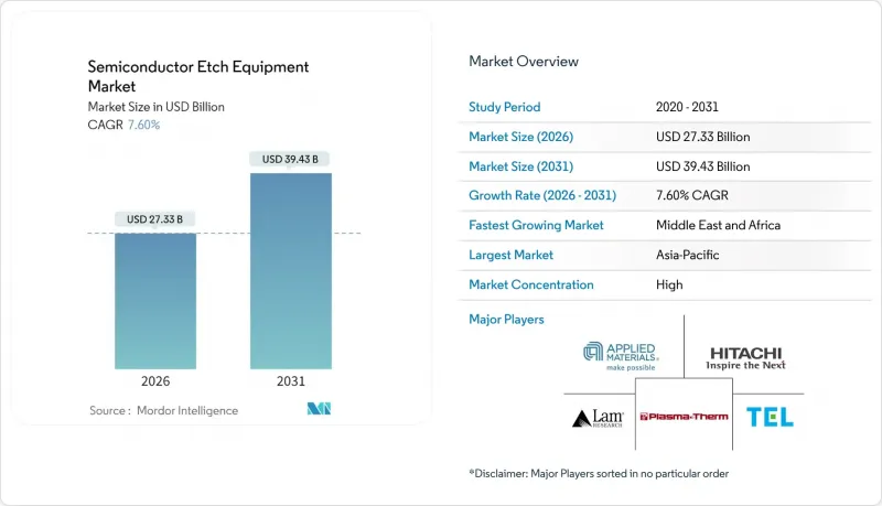
Semiconductor Etch Equipment - Market Share Analysis, Industry Trends & Statistics, Growth Forecasts (2026 - 2031)
The semiconductor etch equipment market is expected to grow from USD 25.4 billion in 2025 to USD 27.33 billion in 2026 and is forecast to reach USD 39.43 billion by 2031 at 7.60% CAGR over 2026-2031.
This growth reflects sustained capital spending at advanced process nodes, accelerating adoption of gate-all-around transistors, and wider deployment of heterogeneous integration. Rising artificial-intelligence workloads, expanding electric-vehicle production, and national subsidy programs continue to enlarge the addressable base of installed tools, while persistent helium shortages and export-control rules shape investment timing. Logic and microprocessor fabs remain the most equipment-intensive customers, commanding the largest share of shipments, yet high-bandwidth-memory and advanced-packaging lines post the fastest unit growth as data-center operators require higher bandwidth and improved energy efficiency. Atomic-layer-etch platforms record the highest revenue momentum, but inductively coupled plasma tools still anchor high-volume manufacturing lines because of their throughput and chemistry flexibility. Regionally, Asia-Pacific dominates installed capacity, although subsidy-backed fab projects in North America, Europe, and the Middle East steadily diversify the geographic footprint of the semiconductor etch equipment market.
Global Semiconductor Etch Equipment Market Trends and Insights
Equipment miniaturization below 3 nm node
Shrinking logic geometries compel fabs to adopt etchers that deliver atomic-level dimensional control while limiting plasma-induced damage. Samsung's volume ramp of 3 nm gate-all-around devices and TSMC's N2 process qualification amplify immediate demand for atomic-layer-etch chambers that remove material one monolayer at a time. Applied Materials and Lam Research deploy proprietary pulsed-plasma cycles and in-situ metrology to meet sub-nanometer variability budgets, which strengthens their competitive moat as smaller vendors struggle to fund similar R&D. Intel's 18A roadmap extends the requirement for even tighter profile control, anchoring multi-year visibility for suppliers positioned on these nodes. As node migration pushes film stacks toward high-k dielectrics and ruthenium barriers, differentiated chemistries further raise switching costs for fabs and reinforce pricing power for leading toolmakers.
Rapid capacity build in Chinese foundries
Chinese logic and specialty foundries added roughly 200,000 wafer starts per month in 2024, equal to nearly 15% of global build-out, despite broader cyclical softness. Government equity injections and advantageous land leasing accelerate greenfield construction, while export-license uncertainty prompts operators to front-load equipment receipts. Domestic champions such as NAURA supply an expanding share of mid-node etchers, but tier-one foreign vendors still capture most advanced-node orders. Stockpiling ahead of anticipated rule changes keeps quarterly bookings elevated even during industry pauses, cushioning the semiconductor etch equipment market against typical downturns.
Cyclical cap-ex swings in memory sector
Memory producers periodically slash equipment budgets to correct overcapacity. SK Hynix, Micron, and Samsung cut etch purchases by nearly 25% in early 2024 following a supply glut, dampening quarterly tool shipments. Because 3D NAND stacks require more than 200 etch passes, each spending pause disproportionately weights the revenue of etch suppliers. Although the logic segment provides a partial offset, the amplitude of memory cycles injects volatility into production planning for equipment vendors.
Other drivers and restraints analyzed in the detailed report include:
- Transition to gate-all-around transistors
- 300 mm-to-200 mm retrofit demand in power devices
- Helium and rare-gas supply disruptions
For complete list of drivers and restraints, kindly check the Table Of Contents.
Segment Analysis
Logic and microprocessor fabs accounted for a 36.65% share of the semiconductor etch equipment market size in 2025, securing that primacy by migrating fastest toward sub-3 nm structures. Each new node requires tighter profile control, thereby boosting per-wafer etch spend. Continuous smartphone and data-center refresh cycles reinforce wafer starts, while mixed-signal chips for automotive autonomy add incremental volume. Memory capacity additions remain episodic, but 3D NAND layer counts above 230 sustain deep-trench etch demand. Advanced packaging and high-bandwidth-memory lines, projected to grow at an 8.79% CAGR through 2031, gain from AI accelerators that pair logic dies with stacked DRAM.
Foundry services attract fabless chipmakers seeking risk-sharing models, pushing TSMC to expand CoWoS packaging output to 65,000 wafers per month by late 2025. Power and discrete devices accelerate as electric-vehicle inverters and fast chargers embed more SiC switches, drawing specialized deep-reactive-ion systems. MEMS and sensor makers exploit low-pressure plasma modules for microphone arrays and tire-pressure monitors. Emerging photonic and quantum devices, though presently niche, demand atomic-level etch selectivity, offering new avenues for supplier differentiation.
Inductively coupled plasma tools delivered 33.25% of 2025 revenue, cementing their status as the backbone of high-volume fabs. Their broad chemistry range allows one platform to tackle polysilicon, high-k dielectrics, and metal gates, simplifying line maintenance. Reactive-ion systems retain service in trailing nodes where aspect-ratio constraints are modest. Deep-RIE tools capture specialty segments such as MEMS and through-silicon-vias, commanding premium margins for their niche capability.
Atomic-layer-etch platforms record the highest growth at a 9.01% CAGR as the semiconductor etch equipment market pivots toward angstrom-level control. Applied Materials advertises pulsed radio-frequency steps that remove a single monolayer per cycle. High-aspect-ratio modules tackle 3D NAND trenches exceeding 60:1, where sidewall bowing can cripple cell efficiency. Wet-bench systems persist for isotropic cleans and pre-bond surface prep, yet their total share erodes as plasma chemistries grow gentler and more selective.
The Semiconductor Etch Equipment Market Report is Segmented by Application (Logic/MPU, Memory, and More), Equipment Type (Reactive Ion Etcher, ICP Etcher, Deep RIE, Wet Etch Systems, High-Aspect-Ratio Etch, and Atomic Layer Etch), Etching Technology (Dry Etch and Wet Etch), Process Type (Front-End-Of-Line (FEOL) Etching and Back-End-Of-Line (BEOL) Etching), and Geography. The Market Forecasts are Provided in Terms of Value (USD).
Geography Analysis
Asia-Pacific generated 70.85% of 2025 revenue as Taiwan, South Korea, and mainland China sustained multi-billion-dollar capacity additions. TSMC's CoWoS expansion to 65,000 wafers per month illustrates regional leadership in advanced packaging, while Samsung and SK Hynix cycles in DRAM and NAND continue to command large etch volumes. Domestic Chinese vendors climb the learning curve rapidly; NAURA's 44% profit growth and move into the global top-six underlines this progress.
North America's share is buoyed by CHIPS Act incentives exceeding USD 50 billion. Intel's USD 20 billion Ohio build and TSMC's Arizona site pull large multi-chamber etch orders, diversifying supplier backlog away from sole reliance on Asia. European Chips Act funds steer projects in Germany, France, and Ireland, extending visibility for equipment shipments through decade-end.
The Middle East and Africa record the fastest projected CAGR at 10.74% as governments seek strategic autonomy. Saudi Arabia's NEOM campus and the United Arab Emirates' clean-room programs commit to pilot lines that import turnkey etch modules. Infrastructure gaps and talent shortages remain hurdles, yet sustained public funding attracts global suppliers, further widening the geographic base of the semiconductor etch equipment market.
- Applied Materials, Inc.
- Lam Research Corp.
- Tokyo Electron Ltd.
- Hitachi High-Tech Corp.
- Plasma-Therm LLC
- ASM International N.V.
- NAURA Technology Group Co., Ltd.
- Oxford Instruments Plasma Technology Ltd.
- SPTS Technologies Ltd. (KLA)
- ULVAC, Inc.
- Veeco Instruments Inc.
- SAMCO Inc.
- Advanced Micro-Fabrication Equipment Inc. (AMEC)
- Mattson Technology Inc.
- GlobalFoundries Inc. (In-house Tools)
- Suzhou Ruidow Technology Co., Ltd.
- PVA TePla AG
- CORIAL SAS
- Trion Technology Inc.
- Tescan Orsay Holding a.s.
Additional Benefits:
- The market estimate (ME) sheet in Excel format
- 3 months of analyst support
TABLE OF CONTENTS
1 INTRODUCTION
- 1.1 Study Assumptions and Market Definition
- 1.2 Scope of the Study
2 RESEARCH METHODOLOGY
3 EXECUTIVE SUMMARY
4 MARKET LANDSCAPE
- 4.1 Market Overview
- 4.2 Impact of Macroeconomic Factors
- 4.3 Industry Supply Chain Analysis
- 4.4 Market Drivers
- 4.4.1 Equipment miniaturization below 3 nm node
- 4.4.2 Rapid capacity-build in Chinese foundries
- 4.4.3 Transition to gate-all-around (GAA) transistors
- 4.4.4 300 mm-to-200 mm retrofit demand in power devices
- 4.4.5 U.S. and EU fab-subsidy outlays (CHIPS Acts)
- 4.4.6 Heterogeneous integration and advanced packaging
- 4.5 Market Restraints
- 4.5.1 Cyclical cap-ex swings in memory sector
- 4.5.2 Helium and rare-gas supply disruptions
- 4.5.3 Rising tool average selling prices vs ROI
- 4.5.4 Escalating export-control compliance costs
- 4.6 Regulatory Landscape
- 4.7 Technological Outlook
- 4.8 Porter's Five Forces Analysis
- 4.8.1 Threat of New Entrants
- 4.8.2 Bargaining Power of Buyers/Consumers
- 4.8.3 Bargaining Power of Suppliers
- 4.8.4 Threat of Substitute Products
- 4.8.5 Intensity of Competitive Rivalry
5 MARKET SIZE AND GROWTH FORECASTS (VALUE)
- 5.1 By Application
- 5.1.1 Logic / MPU
- 5.1.2 Memory
- 5.1.3 Foundry Services
- 5.1.4 Power and Discrete Devices
- 5.1.5 MEMS and Sensors
- 5.1.6 Advanced Packaging / HBM
- 5.1.7 Others
- 5.2 By Equipment Type
- 5.2.1 Reactive Ion Etcher (RIE)
- 5.2.2 Inductively Coupled Plasma (ICP) Etcher
- 5.2.3 Deep RIE (DRIE)
- 5.2.4 Wet Etch Systems
- 5.2.5 High-Aspect-Ratio Etch (HARP)
- 5.2.6 Atomic Layer Etch (ALE)
- 5.3 By Etching Technology
- 5.3.1 Dry Etch
- 5.3.2 Wet Etch
- 5.4 By Process Type
- 5.4.1 Front-End-of-Line (FEOL) Etching
- 5.4.2 Back-End-of-Line (BEOL) Etching
- 5.5 Geography
- 5.5.1 North America
- 5.5.1.1 United States
- 5.5.1.2 Canada
- 5.5.1.3 Mexico
- 5.5.2 South America
- 5.5.2.1 Brazil
- 5.5.2.2 Argentina
- 5.5.2.3 Rest of South America
- 5.5.3 Europe
- 5.5.3.1 Germany
- 5.5.3.2 United Kingdom
- 5.5.3.3 France
- 5.5.3.4 Italy
- 5.5.3.5 Spain
- 5.5.3.6 Russia
- 5.5.3.7 Rest of Europe
- 5.5.4 Asia-Pacific
- 5.5.4.1 China
- 5.5.4.2 Japan
- 5.5.4.3 India
- 5.5.4.4 South Korea
- 5.5.4.5 South-East Asia
- 5.5.4.6 Rest of Asia-Pacific
- 5.5.5 Middle East and Africa
- 5.5.5.1 Middle East
- 5.5.5.1.1 Saudi Arabia
- 5.5.5.1.2 United Arab Emirates
- 5.5.5.1.3 Turkey
- 5.5.5.1.4 Rest of Middle East
- 5.5.5.2 Africa
- 5.5.5.2.1 South Africa
- 5.5.5.2.2 Nigeria
- 5.5.5.2.3 Rest of Africa
- 5.5.5.1 Middle East
- 5.5.1 North America
6 COMPETITIVE LANDSCAPE
- 6.1 Market Concentration
- 6.2 Strategic Moves
- 6.3 Market Share Analysis
- 6.4 Company Profiles {(includes Global level Overview, Market level overview, Core Segments, Financials as available, Strategic Information, Market Rank/Share for key companies, Products and Services, and Recent Developments)}
- 6.4.1 Applied Materials, Inc.
- 6.4.2 Lam Research Corp.
- 6.4.3 Tokyo Electron Ltd.
- 6.4.4 Hitachi High-Tech Corp.
- 6.4.5 Plasma-Therm LLC
- 6.4.6 ASM International N.V.
- 6.4.7 NAURA Technology Group Co., Ltd.
- 6.4.8 Oxford Instruments Plasma Technology Ltd.
- 6.4.9 SPTS Technologies Ltd. (KLA)
- 6.4.10 ULVAC, Inc.
- 6.4.11 Veeco Instruments Inc.
- 6.4.12 SAMCO Inc.
- 6.4.13 Advanced Micro-Fabrication Equipment Inc. (AMEC)
- 6.4.14 Mattson Technology Inc.
- 6.4.15 GlobalFoundries Inc. (In-house Tools)
- 6.4.16 Suzhou Ruidow Technology Co., Ltd.
- 6.4.17 PVA TePla AG
- 6.4.18 CORIAL SAS
- 6.4.19 Trion Technology Inc.
- 6.4.20 Tescan Orsay Holding a.s.
7 MARKET OPPORTUNITIES AND FUTURE OUTLOOK
- 7.1 White-space and Unmet-Need Assessment

