
PUBLISHER: Mordor Intelligence | PRODUCT CODE: 2035094

PUBLISHER: Mordor Intelligence | PRODUCT CODE: 2035094
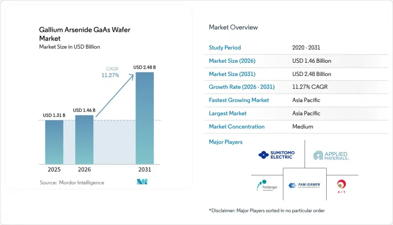
Gallium Arsenide GaAs Wafer - Market Share Analysis, Industry Trends & Statistics, Growth Forecasts (2026 - 2031)
Gallium arsenide wafer market size in 2026 is estimated at USD 1.46 billion, growing from 2025 value of USD 1.31 billion with 2031 projections showing USD 2.48 billion, growing at 11.27% CAGR over 2026-2031.
Robust demand for high-frequency radio modules, optoelectronic emitters, and defense-grade radar devices keeps Gallium arsenide substrates firmly positioned where silicon performance plateaus. Large telecom operators are refreshing network hardware to 5G standards, compelling front-end module suppliers to specify GaAs power amplifiers that outperform CMOS at millimeter-wave bands. In parallel, data-center operators adopt VCSEL arrays on GaAs to move 400G and 800G traffic with lower latency, while micro-LED innovators count on GaAs epi uniformity to scale augmented-reality headsets. Investment patterns confirm that Asia-Pacific fabs leverage vertical integration and cost advantages to supply global customers, even as North America rings-fences critical military demand for radiation-hardened wafers. Breakthrough concepts such as remote epitaxy promise to recycle substrates, hinting at future shifts in GaAs consumption economics without dampening near-term demand.
Global Gallium Arsenide GaAs Wafer Market Trends and Insights
5G Infrastructure Roll-out Fuels GaAs RF Demand
Telecom operators are deploying dense 5G macro- and small-cell sites that require power amplifiers sustaining linear output well above 28 GHz, where silicon LDMOS falters. Gallium arsenide wafers deliver electron mobility around 8,500 cm2/V*s, enabling efficient front-end modules that preserve signal integrity in massive-MIMO arrays for urban coverage. Network vendors lock multiyear supply contracts with vertically integrated GaAs houses, converting 4G hardware refresh cycles into predictable demand through 2027.
Optoelectronic Device Boom (VCSELs, Lasers)
Hyperscale data centers move to 400G and 800G optics that rely on GaAs-based VCSEL arrays for lower latency and power draw. Smartphone makers embed 3D-sensing VCSELs in biometric modules, while automotive OEMs adopt GaAs lasers for LiDAR. Epitaxial regrowth advances improve thermal dissipation, extending device lifetimes and sustaining premium wafer ASPs.
High Production Cost vs Si and SiC
GaAs crystal pulling needs pressurized arsenic atmospheres and toxic-gas handling that raise CapEx and Opex above silicon. Smaller 4-inch and 6-inch formats cannot match the die-per-wafer economics of 300 mm silicon, limiting GaAs uptake in price-sensitive consumer gadgets.
Other drivers and restraints analyzed in the detailed report include:
- Aerospace and Defense Uptake for High-Frequency Radar
- Asian Epitaxy Capacity Boosts Supply and Lowers ASP
- Gallium Supply Concentration and Export Controls
For complete list of drivers and restraints, kindly check the Table Of Contents.
Segment Analysis
RF electronics held 43.65% revenue in 2025 as power amplifiers and switches remain core to 5G infrastructure upgrades. This portion of the Gallium arsenide wafer market size is forecast to climb steadily alongside small-cell densification plans. Photonic and imaging devices, propelled by VCSEL interconnects and AR/VR optics, are set to outpace all other uses at 13.25% CAGR, thereby reshaping future volumes of the Gallium arsenide wafer market.
Cross-segment pull-through emerges as handset makers integrate VCSEL-based face ID modules, boosting both photonics and RF volume on common 6-inch epi lines. Solar cells on GaAs remain a niche for spacecraft, yet new heterointegration concepts could push multi-junction designs into terrestrial concentrator arrays.
Four-inch substrates still command 35.85% revenue thanks to mature tooling, but capacity announcements reveal that 6-inch lines will absorb most incremental demand at 12.85% CAGR. The shift improves die counts per run and spreads fixed costs, nudging the overall Gallium arsenide wafer market toward lower ASPs.
Equipment vendors tackle thermal-gradient control and arsenic vapor management to scale beyond 6 inches. Early 8-inch pilot runs show promise yet require further defect reduction before commercial deployment.
The Gallium Arsenide (GaAs) Wafer Market Report is Segmented by Application (Radio-Frequency Electronics, and More), Wafer Diameter (2 Inch, 3 Inch, 4 Inch, and More), Growth Technology (LEC, VGF, and More), End-Use Industry (Telecom and 5G Infrastructure, and More), Conductivity Type (Semi-Insulating GaAs, Semi-Conducting GaAs), and Geography (North America, and More). The Market Forecasts are Provided in Terms of Value (USD).
Geography Analysis
Asia-Pacific held 60.10% of the Gallium arsenide wafer market in 2025 thanks to clustered epitaxial lines, a deep subcontract base, and state-backed 5G build-outs. Government incentives help mainland China expand compound-semiconductor fabs, while Taiwan and South Korea provide foundry and equipment synergies that reinforce supply diversity.
North America ranks second, anchored by aerospace and defense demand requiring secure on-shore production. Recent CHIPS Act incentives finance new crystal-growth reactors and cleanrooms dedicated to semi-insulating material for radar and satellite programs, cementing long-term domestic supply.
Europe retains strength in automotive and industrial automation. Tier-1 suppliers source GaAs power devices to support ADAS radar and factory sensing, while stringent environmental directives spur circular-economy research on wafer reclamation. Coordinated EU funding backs pilot lines for 150 mm compound-semiconductor substrates, seeking to narrow the capacity gap with Asia.
- AXT Inc.
- China Crystal Technologies Co. Ltd.
- Freiberger Compound Materials GmbH
- Semiconductor Wafer Inc.
- Sumitomo Electric Industries, Ltd.
- Xiamen Powerway Advanced Material Co., Ltd.
- Wafer Technology Ltd.
- Vital Materials Co., Ltd.
- DOWA Electronics Materials Co., Ltd.
- American Elements, Inc.
- IQE plc
- WIN Semiconductors Corp.
- Advanced Wireless Semiconductor Co.
- Visual Photonics Epitaxy Co., Ltd. (VPEC)
- IntelliEPI, Inc.
- Global Communication Semiconductors, LLC
- Roditi Ltd.
- Veeco Instruments Inc.
- Applied Materials, Inc.
- AIXTRON SE
Additional Benefits:
- The market estimate (ME) sheet in Excel format
- 3 months of analyst support
TABLE OF CONTENTS
1 INTRODUCTION
- 1.1 Study Assumptions and Market Definition
- 1.2 Scope of the Study
2 RESEARCH METHODOLOGY
3 EXECUTIVE SUMMARY
4 MARKET LANDSCAPE
- 4.1 Market Overview
- 4.2 Market Drivers
- 4.2.1 5G infrastructure roll-out fuels GaAs RF demand
- 4.2.2 Optoelectronic device boom (VCSELs, lasers)
- 4.2.3 Aerospace and defense uptake for high-freq radar
- 4.2.4 Asian epitaxy capacity boosts supply and lowers ASP
- 4.2.5 Micro-LED adoption in AR/VR wearables
- 4.2.6 Remote-epitaxy substrate reuse cuts wafer cost
- 4.3 Market Restraints
- 4.3.1 High production cost vs Si and SiC
- 4.3.2 Gallium supply concentration and export controls
- 4.3.3 GaN and SiC competition in RF / power
- 4.3.4 Environmental and safety compliance
- 4.4 Industry Value Chain Analysis
- 4.5 Regulatory Landscape
- 4.6 Technological Outlook
- 4.7 Porter's Five Forces Analysis
- 4.7.1 Bargaining Power of Suppliers
- 4.7.2 Bargaining Power of Buyers
- 4.7.3 Threat of New Entrants
- 4.7.4 Threat of Substitute Products
- 4.7.5 Intensity of Competitive Rivalry
5 MARKET SIZE AND GROWTH FORECASTS (VALUE)
- 5.1 By Application
- 5.1.1 Radio-Frequency Electronics
- 5.1.2 Optical and IR LEDs
- 5.1.3 Photovoltaic / Solar Cells
- 5.1.4 Photonic and Imaging Devices
- 5.1.5 Other Applications
- 5.2 By Wafer Diameter
- 5.2.1 2 inch (50 mm)
- 5.2.2 3 inch (76 mm)
- 5.2.3 4 inch (100 mm)
- 5.2.4 6 inch (150 mm)
- 5.2.5 8 inch (200 mm) and Above
- 5.3 By Growth Technology
- 5.3.1 Liquid-Encapsulated Czochralski (LEC)
- 5.3.2 Vertical Gradient Freeze (VGF)
- 5.3.3 Horizontal Bridgman (HB)
- 5.3.4 Molecular Beam Epitaxy (MBE)
- 5.3.5 Metal-Organic CVD (MOCVD)
- 5.4 By End-Use Industry
- 5.4.1 Telecom and 5G Infrastructure
- 5.4.2 Consumer Electronics
- 5.4.3 Aerospace and Defense
- 5.4.4 Automotive (ADAS, EV)
- 5.4.5 Industrial and Energy
- 5.5 By Conductivity Type
- 5.5.1 Semi-insulating GaAs
- 5.5.2 Semi-conducting GaAs (n-/p-type)
- 5.6 By Geography
- 5.6.1 North America
- 5.6.1.1 United States
- 5.6.1.2 Canada
- 5.6.1.3 Mexico
- 5.6.2 South America
- 5.6.2.1 Brazil
- 5.6.2.2 Argentina
- 5.6.2.3 Rest of South America
- 5.6.3 Europe
- 5.6.3.1 Germany
- 5.6.3.2 United Kingdom
- 5.6.3.3 France
- 5.6.3.4 Italy
- 5.6.3.5 Rest of Europe
- 5.6.4 Asia-Pacific
- 5.6.4.1 China
- 5.6.4.2 Japan
- 5.6.4.3 South Korea
- 5.6.4.4 India
- 5.6.4.5 Rest of Asia-Pacific
- 5.6.5 Middle East
- 5.6.5.1 Saudi Arabia
- 5.6.5.2 United Arab Emirates
- 5.6.5.3 Rest of Middle East
- 5.6.6 Africa
- 5.6.6.1 South Africa
- 5.6.6.2 Rest of Africa
- 5.6.1 North America
6 COMPETITIVE LANDSCAPE
- 6.1 Market Concentration
- 6.2 Strategic Moves
- 6.3 Market Share Analysis
- 6.4 Company Profiles (includes Global level Overview, Market level overview, Core Segments, Financials as available, Strategic Information, Market Rank/Share, Products and Services, Recent Developments)
- 6.4.1 AXT Inc.
- 6.4.2 China Crystal Technologies Co. Ltd.
- 6.4.3 Freiberger Compound Materials GmbH
- 6.4.4 Semiconductor Wafer Inc.
- 6.4.5 Sumitomo Electric Industries, Ltd.
- 6.4.6 Xiamen Powerway Advanced Material Co., Ltd.
- 6.4.7 Wafer Technology Ltd.
- 6.4.8 Vital Materials Co., Ltd.
- 6.4.9 DOWA Electronics Materials Co., Ltd.
- 6.4.10 American Elements, Inc.
- 6.4.11 IQE plc
- 6.4.12 WIN Semiconductors Corp.
- 6.4.13 Advanced Wireless Semiconductor Co.
- 6.4.14 Visual Photonics Epitaxy Co., Ltd. (VPEC)
- 6.4.15 IntelliEPI, Inc.
- 6.4.16 Global Communication Semiconductors, LLC
- 6.4.17 Roditi Ltd.
- 6.4.18 Veeco Instruments Inc.
- 6.4.19 Applied Materials, Inc.
- 6.4.20 AIXTRON SE
7 MARKET OPPORTUNITIES AND FUTURE OUTLOOK
- 7.1 White-space and Unmet-need Assessment

