
PUBLISHER: Mordor Intelligence | PRODUCT CODE: 2044043

PUBLISHER: Mordor Intelligence | PRODUCT CODE: 2044043
Asia-Pacific LED Epitaxy MOCVD Equipment - Market Share Analysis, Industry Trends & Statistics, Growth Forecasts (2026 - 2031)
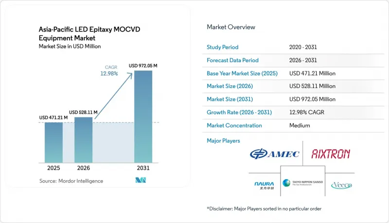
The Asia-Pacific LED epitaxy MOCVD equipment market size is projected to be USD 471.21 million in 2025, USD 528.11 million in 2026, and reach USD 972.05 million by 2031, growing at a CAGR of 12.98% from 2026 to 2031.
Robust state incentives for domestic semiconductor tools, the pivot toward mini-LED and micro-LED displays, and the shift to larger GaN wafers are together accelerating capital spending across China, Taiwan, Japan, and South Korea. Local equipment vendors are capitalizing on Beijing's mandate that at least half of new semiconductor tools come from domestic suppliers, while display makers are qualifying advanced showerhead reactors to meet tight wavelength-binning targets. Gallium export controls are reinforcing regional self-reliance, driving long-term supply-chain realignment, and expanding addressable demand for indigenous precursor purification. At the same time, AI-driven in-situ metrology is becoming standard on new tools, cutting defect density and shortening root-cause analysis cycles. Refurbishment programs are widening access to mature reactors for Tier-2 fabs, enabling incremental capacity additions without full capital outlays.
Asia-Pacific LED Epitaxy MOCVD Equipment Market Trends and Insights
Government Subsidies for Compound-Semiconductor Fabs in China
China's Big Fund Phase 3 set aside USD 47.5 billion to accelerate domestic tool adoption, with quotas stipulating that half of new equipment purchases come from local vendors. Domestic penetration rose from 25% in 2024 to 35% in 2025, directly lifting shipments for NAURA Technology Group and Advanced Micro-Fabrication Equipment Inc. Provincial tax holidays and subsidized industrial parks have cut effective fab capex by up to 30%, unlocking incremental orders for multi-wafer reactors. Gallium resource dominance further aligns state incentives with supply-chain localization. Neighboring Malaysian and Vietnamese LED makers are already sourcing Chinese tools to qualify for reduced-tariff trade corridors, reinforcing the driver's regional spill-over effect.
Surge in Demand for Mini and Micro-LED Displays
Omdia projects global micro-LED display revenue to double between 2025 and 2026, then scale to USD 6.8 billion by 2032. Mini-LED TV shipments climbed 100% year-over-year to 8.2 million units in 2024, lifting demand for narrow-binning epitaxial wafers. Display suppliers now require +-2.5 nm wavelength tolerance, prompting migration from planetary to showerhead reactors. Veeco's Lumina series logged repeat orders in 2026 for indium-phosphide lasers that support AI-server optical links, highlighting cross-market synergies. Although chip-on-board backlighting faces oversupply risk, adoption in automotive dashboards and augmented-reality headsets is absorbing idle epi capacity.
High Capital Cost of Multi-Wafer MOCVD Tools
State-of-the-art 200 mm batch reactors carry USD 3-5 million price tags, a hurdle for fabs with annual sales below USD 50 million. Although Alliance MOCVD and Heraeus Covantics offer 30-40% discounts on refurbished 100 mm equipment, availability of newer 150 mm or 200 mm tools in the secondary market is limited. Long four-to-six-year payback periods discourage greenfield investment when demand visibility narrows. Leasing structures are emerging in Taiwan and Japan, yet mainland China lenders remain cautious, keeping financing channels constrained. The capex burden therefore delays technology transitions and tempers short-term shipment spikes for the Asia-Pacific LED epitaxy MOCVD equipment market.
Other drivers and restraints analyzed in the detailed report include:
- Shift to 150 mm and 200 mm GaN Wafers for Cost Reduction
- Increasing Adoption of UV-C LED Disinfection Systems
- Oversupply Risk in LED Backlighting Market
For complete list of drivers and restraints, kindly check the Table Of Contents.
Segment Analysis
GaN platforms anchored 68.86% of the market share in 2025, thanks to entrenched use in general lighting, backlighting, and automotive headlamps. Mature precursor ecosystems and substrate optionality keep GaN die costs competitive, reinforcing the Asia-Pacific LED epitaxy MOCVD equipment market's installed base advantage. Taiwan Semiconductor Manufacturing Company's USD 2 billion gallium recycling program is further insulating GaN supply from export volatility. AlGaN UV-C devices sit at a smaller baseline yet carry a 13.24% forecast CAGR, buoyed by stringent hygiene mandates in water-treatment and healthcare facilities. Tight emission regulations in Europe and North America are already spurring municipal retrofit projects, translating into firm tool orders for high-temperature reactors that can sustain >1,100 °C growth windows.
Supply-chain specialization is deepening. Chinese and Taiwanese foundries are ramping AlGaN epi pilot lines, leveraging AI-driven in-situ metrology to tackle high threading-dislocation density. Western vendors, meanwhile, are redirecting arsenide-phosphide reactor roadmaps toward power electronics and solar concentrator markets, allowing domestic APAC players to consolidate GaN LED share. The Asia-Pacific LED epitaxy MOCVD equipment industry therefore expects GaN to remain the revenue anchor, while AlGaN provides the incremental growth zest that lifts blended margins.
In 2025, the 150 mm segment accounted for 46.39% of the market share, reflecting its long-standing role in volume LED manufacturing. Yet the 200 mm and above category is charted to post a 13.63% CAGR, as larger substrates lower per-die cost and align with mainstream silicon fab logistics. Utilization improvements stem from smaller edge exclusion zones, which drop from near 20% on 100 mm wafers to roughly 8-10% on 200 mm lots, enhancing effective capital-per-square-centimeter economics. Veeco's Propel platform, capable of seamless 300 mm transitions, illustrates equipment makers' push to future-proof customer roadmaps.
The transition, however, is uneven. Japanese and Taiwanese IDMs have re-purposed legacy DRAM cleanrooms for GaN epi, minimizing incremental infrastructure spend, whereas many mainland Chinese fabs must finance entirely new bulk-gas and abatement systems for 200 mm readiness. Sapphire cost and defectivity currently limit some UV-C and laser applications to 150 mm, preserving a multi-diameter ecosystem. Overall, migration dynamics underscore how wafer-size shifts can swing capex timing for the Asia-Pacific LED epitaxy MOCVD equipment market.
The Asia-Pacific LED Epitaxy MOCVD Equipment Market Report is Segmented by LED Material System (GaN-Based LED Epitaxy Systems, and More), Wafer Size Capability (Up To 100mm, 150mm, and 200mm and Above), Reactor Configuration (Planetary Reactors, and Showerhead Reactors), End User (Integrated LED Manufacturers, and Epitaxy Foundries and Merchant Epi Suppliers), and Country. The Market Forecasts are Provided in Terms of Value (USD).
List of Companies Covered in this Report:
- AIXTRON SE
- Veeco Instruments Inc.
- Advanced Micro-Fabrication Equipment Inc. (AMEC)
- NAURA Technology Group Co. Ltd.
- Taiyo Nippon Sanso Corporation
- ASM International N.V.
- Tokyo Electron Ltd.
- Applied Materials Inc.
- topecsh Co. Ltd.
- CVD Equipment Corporation
- NuFlare Technology Inc.
- Jusung Engineering Co. Ltd.
- Element 3-5 GmbH
- Alliance MOCVD LLC
- Suzhou Powerway Wafer Co. Ltd.
- Sanan Optoelectronics Co. Ltd.
- Epistar Corporation
- Silan Azure Co. Ltd.
Additional Benefits:
- The market estimate (ME) sheet in Excel format
- 3 months of analyst support
TABLE OF CONTENTS
1 INTRODUCTION
- 1.1 Study Assumptions and Market Definition
- 1.2 Scope of the Study
2 RESEARCH METHODOLOGY
3 EXECUTIVE SUMMARY
4 MARKET LANDSCAPE
- 4.1 Market Overview
- 4.2 Market Drivers
- 4.2.1 Government Subsidies for Compound-Semiconductor Fabs in China
- 4.2.2 Surge in Demand for Mini and Micro-LED Displays
- 4.2.3 Shift to 150 mm and 200 mm GaN Wafers for Cost Reduction
- 4.2.4 Increasing Adoption of UV-C LED Disinfection Systems
- 4.2.5 AI-Driven In-Situ Metrology Integration Reducing Yield Loss
- 4.2.6 Circular Reactor Refurbishment Programs Lowering CapEx
- 4.3 Market Restraints
- 4.3.1 High Capital Cost of Multi-Wafer MOCVD Tools
- 4.3.2 Oversupply Risk in LED Backlighting Market
- 4.3.3 Volatile Trimethylgallium and Ammonia Supply Chains
- 4.3.4 Shortage of Experienced Epitaxy Engineers in Tier-2 Cities
- 4.4 Industry Supply Chain Analysis
- 4.5 Technological Outlook
- 4.6 Regulatory Landscape
- 4.7 Impact of Macroeconomic Factors on the Market
- 4.8 Porter's Five Forces Analysis
- 4.8.1 Threat of New Entrants
- 4.8.2 Bargaining Power of Suppliers
- 4.8.3 Bargaining Power of Buyers
- 4.8.4 Threat of Substitutes
- 4.8.5 Intensity of Competitive Rivalry
5 MARKET SIZE AND GROWTH FORECASTS (VALUE)
- 5.1 By LED Material System
- 5.1.1 GaN-based LED Epitaxy Systems
- 5.1.2 AlGaN UV LED Epitaxy Systems
- 5.1.3 AlInGaP LED Epitaxy Systems
- 5.2 By Wafer Size Capability
- 5.2.1 Upto 100 mm
- 5.2.2 150 mm
- 5.2.3 200 mm and Above
- 5.3 By Reactor Configuration
- 5.3.1 Planetary Reactors
- 5.3.2 Showerhead Reactors
- 5.4 By End User
- 5.4.1 Integrated LED Manufacturers (IDMs)
- 5.4.2 Epitaxy Foundries and Merchant Epi Suppliers
- 5.5 By Country
- 5.5.1 China
- 5.5.2 Japan
- 5.5.3 Taiwan
- 5.5.4 Rest of Asia-Pacific
6 COMPETITIVE LANDSCAPE
- 6.1 Market Concentration
- 6.2 Strategic Moves
- 6.3 Market Share Analysis
- 6.4 Company Profiles (Includes Global Level Overview, Market Level Overview, Core Segments, Financials as Available, Strategic Information, Market Rank/Share, Products and Services, and Recent Developments)
- 6.4.1 AIXTRON SE
- 6.4.2 Veeco Instruments Inc.
- 6.4.3 Advanced Micro-Fabrication Equipment Inc. (AMEC)
- 6.4.4 NAURA Technology Group Co. Ltd.
- 6.4.5 Taiyo Nippon Sanso Corporation
- 6.4.6 ASM International N.V.
- 6.4.7 Tokyo Electron Ltd.
- 6.4.8 Applied Materials Inc.
- 6.4.9 topecsh Co. Ltd.
- 6.4.10 CVD Equipment Corporation
- 6.4.11 NuFlare Technology Inc.
- 6.4.12 Jusung Engineering Co. Ltd.
- 6.4.13 Element 3-5 GmbH
- 6.4.14 Alliance MOCVD LLC
- 6.4.15 Suzhou Powerway Wafer Co. Ltd.
- 6.4.16 Sanan Optoelectronics Co. Ltd.
- 6.4.17 Epistar Corporation
- 6.4.18 Silan Azure Co. Ltd.
7 MARKET OPPORTUNITIES AND FUTURE OUTLOOK
- 7.1 White-Space and Unmet-Need Assessment

