
PUBLISHER: Mordor Intelligence | PRODUCT CODE: 2044045

PUBLISHER: Mordor Intelligence | PRODUCT CODE: 2044045
Japan LED Epitaxy MOCVD Equipment - Market Share Analysis, Industry Trends & Statistics, Growth Forecasts (2026 - 2031)
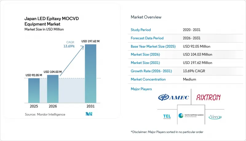
The Japan LED epitaxy MOCVD equipment marketsize is projected to be USD 92.05 million in 2025, USD 104.03 million in 2026, and reach USD 197.62 million by 2031, growing at a CAGR of 13.69% from 2026 to 2031.
An upswing in state subsidies, rapidly rising mini- and micro-LED demand, and the migration of GaN-on-Si power devices to 200 mm and 300 mm wafers underpin this expansion. Tokyo's multi-billion-dollar fiscal-2026 package for semiconductors signals predictable order pipelines for domestic toolmakers, while prototype breakthroughs such as a 10.2% wall-plug-efficiency UV-C LED confirm that Japan-based manufacturers are ready to scale next-generation devices. At the same time, larger wafer formats that lower die cost, and in-situ process control that shortens tool setup times, are sharpening replacement cycles for legacy reactors. Volatility in the yen does inflate imported tool costs, yet corporate net-zero mandates and energy-efficiency retrofits keep capital expenditure directed toward high-efficiency lighting and power electronics.
Japan LED Epitaxy MOCVD Equipment Market Trends and Insights
Surge in Mini and Micro-LED Backlighting Demand
Mini- and micro-LED backlighting for vehicle cockpits and flagship consumer electronics has tightened epitaxy tolerances, pushing suppliers toward sub-nanometer thickness control across 150 mm and 200 mm wafers. Aixtron's G10-AsP platform reports an order-of-magnitude reduction in defect density, aligning with Japan's display majors that require wavelength uniformity for panels exceeding 1,000 ppi. Local R&D partnerships, including Stanley Electric and Kyoto University's photonic-crystal surface-emitting laser program, demonstrate that domestic toolmakers can embed application-specific process recipes. Procurement cycles for these reactors average six months, rewarding vendors that pre-bundle metrology and process-transfer packages. Collectively, these developments raise per-wafer yields and shorten time-to-market for micro-LED modules, directly lifting equipment replacement demand.
Government Subsidies for Domestic Semiconductor Tools
Japan's fiscal-2026 budget allocates JPY 1.23 trillion (USD 7.9 billion) to semiconductors and AI, quadrupling prior-year support and providing predictable, multi-year order visibility for equipment makers. Capital grants flow first to regional clusters hosting TSMC's Kumamoto fab and Rapidus' Hokkaido project, both of which aim for 60% domestic procurement in tool and material spend. Subsidy tranches are linked to technical milestones, lowering the risk of stranded MOCVD assets. The policy also dovetails with tightened export controls that divert Japanese supply away from restricted Chinese demand and toward on-shore or allied fabs, cushioning suppliers against geopolitical swings.
Limited MOCVD Tool Throughput Versus SiC Epitaxy Alternatives
SiC CVD tools deposit thicker layers at higher rates, enabling power fabs to clear more wafers per shift than GaN MOCVD lines. Aixtron shipped its 100th G10-SiC tool in 2025, underscoring how SiC equipment can outpace GaN in high-voltage segments. Modeling studies reveal gas-phase by-product nucleation as a key bottleneck in GaN MOVPE, complicating reactor design. Consequently, several Japanese IDMs cherry-pick GaN only for sub-650 V devices, tempering total reactor demand.
Other drivers and restraints analyzed in the detailed report include:
- Expansion of GaN-on-Si Power Device Supply Chains
- Automotive UV-C LED Adoption for In-Cabin Sterilization
- High Capital Intensity Amid Yen Depreciation
For complete list of drivers and restraints, kindly check the Table Of Contents.
Segment Analysis
The GaN-based LED epitaxy systems segment dominated the Japan LED epitaxy MOCVD equipment market, accounting for 69.09% in 2025, reflecting its entrenched role in white lighting, automotive headlamps, and display backlights. Robust process maturity, broad precursor availability, and standardized planetary reactor recipes keep GaN capital efficient, ensuring stable upgrade cycles. AlGaN UV LED epitaxy systems, while niche in 2025, are tracking a 14.65% CAGR as health-safety regulations and water disinfection projects boost volumes. Equipment buyers value showerhead reactors that curb parasitic aluminum deposition, an essential attribute for sub-280 nm emitters. Concurrently, research into strain-relaxed bulk InGaN aims to displace AlInGaP in red pixels, which would further consolidate spend around GaN family chemistries.
The Japan LED epitaxy MOCVD equipment market share for GaN is also protected by domestic integration moves such as ROHM's plan to bring TSMC GaN recipes in-house. Yet UV suppliers confront higher precursor costs and stricter contamination control, raising barriers for new entrants. Long-term, cross-platform hybrid lines combining MOCVD for active layers with HVPE for thick buffers could cut per-wafer cost, but current pilot results remain limited to 4-inch experiments.
Tools configured for 150 mm wafers held 48.39% of the Japan LED epitaxy MOCVD equipment market share in 2025 because legacy GaN-on-sapphire and GaN-on-Si lines remain profitable at mid-volumes. However, 200 mm and larger systems are registering a 14.38% CAGR as IDMs chase lower die cost and foundries monetize scale economics. The Propel300's qualification for automotive-grade 650 V GaN validates defectivity levels acceptable for power modules, signaling that mass adoption of 300 mm epitaxy is plausible this decade. Pilot programs at academic consortia such as imec further de-risk this transition by publishing >800 V breakdown data on 300 mm QST substrates.
The scale shift is not friction-free. Free-standing GaN substrates above 6 inches remain scarce, compelling many LED makers to stay on 150 mm GaN-on-sapphire. Process migration also involves six-month stabilization windows, during which yield drag can offset wafer-cost gains. Even so, Japan's tool vendors increasingly bundle automated wafer handling and AI-driven run-to-run control that shorten this learning curve.
The Japan LED Epitaxy MOCVD Equipment Market Report is Segmented by LED Material System (GaN-Based LED Epitaxy Systems, and More), Wafer Size Capability (Up To 100mm, 150mm, and 200mm and Above), Reactor Configuration (Planetary Reactors, and Showerhead Reactors), End User (Integrated LED Manufacturers, and Epitaxy Foundries and Merchant Epi Suppliers). The Market Forecasts are Provided in Terms of Value (USD).
List of Companies Covered in this Report:
- Aixtron SE
- Veeco Instruments Inc.
- Advanced Micro-Fabrication Equipment Inc. China
- Beijing NAURA Microelectronics Equipment Co. Ltd.
- Taiyo Nippon Sanso Corporation
- Tokyo Electron Limited
- Kokusai Electric Corporation
- NuFlare Technology Inc.
- Kulicke and Soffa Industries Inc.
- Oxford Instruments plc
- Nichia Corporation
- Rohm Co. Ltd.
- Stanley Electric Co. Ltd.
- Toyoda Gosei Co. Ltd.
- Citizen Electronics Co. Ltd.
- Sharp Corporation
- Panasonic Holdings Corporation
- Sony Semiconductor Manufacturing Corporation
- Sumitomo Electric Industries, Ltd.
Additional Benefits:
- The market estimate (ME) sheet in Excel format
- 3 months of analyst support
TABLE OF CONTENTS
1 INTRODUCTION
- 1.1 Study Assumptions and Market Definition
- 1.2 Scope of the Study
2 RESEARCH METHODOLOGY
3 EXECUTIVE SUMMARY
4 MARKET LANDSCAPE
- 4.1 Market Overview
- 4.2 Market Drivers
- 4.2.1 Surge in Mini and Micro-LED Backlighting Demand
- 4.2.2 Government Subsidies for Domestic Semiconductor Tools
- 4.2.3 Expansion of GaN-on-Si Power Device Supply Chains
- 4.2.4 Automotive UV-C LED Adoption for In-Cabin Sterilization
- 4.2.5 Demand for 150 mm and 200 mm GaN Wafers from Power IC IDMs
- 4.2.6 Corporate Net-Zero Targets Accelerating High-Efficiency Lighting Retrofits
- 4.3 Market Restraints
- 4.3.1 Limited MOCVD Tool Throughput Versus SiC Epitaxy Alternatives
- 4.3.2 High Capital Intensity Amid Yen Depreciation
- 4.3.3 Supply Chain Concentration in China for Key MOCVD Components
- 4.3.4 Slow Qualification Cycles at Japanese Automotive OEMs
- 4.4 Industry Supply Chain Analysis
- 4.5 Technological Outlook
- 4.6 Regulatory Landscape
- 4.7 Impact of Macroeconomic Factors on the Market
- 4.8 Porter's Five Forces Analysis
- 4.8.1 Threat of New Entrants
- 4.8.2 Bargaining Power of Suppliers
- 4.8.3 Bargaining Power of Buyers
- 4.8.4 Threat of Substitutes
- 4.8.5 Intensity of Competitive Rivalry
5 MARKET SIZE AND GROWTH FORECASTS (VALUE)
- 5.1 By LED Material System
- 5.1.1 GaN-based LED Epitaxy Systems
- 5.1.2 AlGaN UV LED Epitaxy Systems
- 5.1.3 AlInGaP LED Epitaxy Systems
- 5.2 By Wafer Size Capability
- 5.2.1 Upto 100 mm
- 5.2.2 150 mm
- 5.2.3 200 mm and Above
- 5.3 By Reactor Configuration
- 5.3.1 Planetary Reactors
- 5.3.2 Showerhead Reactors
- 5.4 By End User
- 5.4.1 Integrated LED Manufacturers (IDMs)
- 5.4.2 Epitaxy Foundries and Merchant Epi Suppliers
6 COMPETITIVE LANDSCAPE
- 6.1 Market Concentration
- 6.2 Strategic Moves
- 6.3 Market Share Analysis
- 6.4 Company Profiles (Includes Global Level Overview, Market Level Overview, Core Segments, Financials as Available, Strategic Information, Market Rank/Share, Products and Services, and Recent Developments)
- 6.4.1 Aixtron SE
- 6.4.2 Veeco Instruments Inc.
- 6.4.3 Advanced Micro-Fabrication Equipment Inc. China
- 6.4.4 Beijing NAURA Microelectronics Equipment Co. Ltd.
- 6.4.5 Taiyo Nippon Sanso Corporation
- 6.4.6 Tokyo Electron Limited
- 6.4.7 Kokusai Electric Corporation
- 6.4.8 NuFlare Technology Inc.
- 6.4.9 Kulicke and Soffa Industries Inc.
- 6.4.10 Oxford Instruments plc
- 6.4.11 Nichia Corporation
- 6.4.12 Rohm Co. Ltd.
- 6.4.13 Stanley Electric Co. Ltd.
- 6.4.14 Toyoda Gosei Co. Ltd.
- 6.4.15 Citizen Electronics Co. Ltd.
- 6.4.16 Sharp Corporation
- 6.4.17 Panasonic Holdings Corporation
- 6.4.18 Sony Semiconductor Manufacturing Corporation
- 6.4.19 Sumitomo Electric Industries, Ltd.
7 MARKET OPPORTUNITIES AND FUTURE OUTLOOK
- 7.1 White-space and Unmet-Need Assessment

