
PUBLISHER: Mordor Intelligence | PRODUCT CODE: 2044055

PUBLISHER: Mordor Intelligence | PRODUCT CODE: 2044055
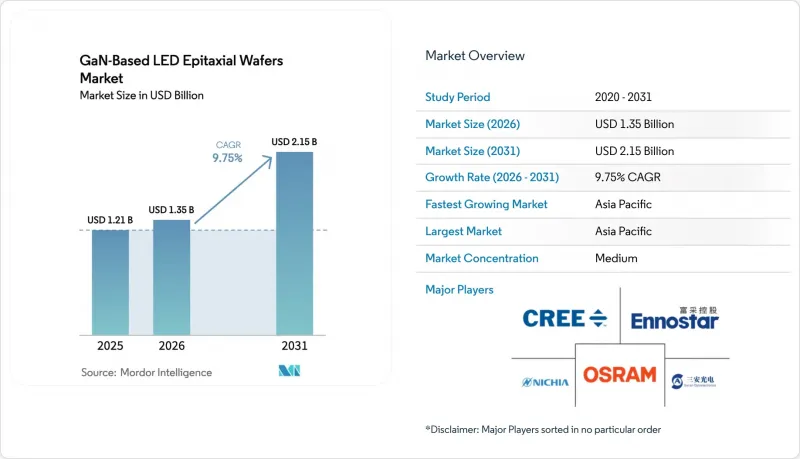
GaN-Based LED Epitaxial Wafers - Market Share Analysis, Industry Trends & Statistics, Growth Forecasts (2026 - 2031)
The GaN-based LED epitaxial wafers market size is expected to increase from USD 1.35 billion in 2026 to USD 2.15 billion by 2031, growing at a CAGR of 9.75% over 2026-2031.
Demand is rising as metal-organic chemical vapor deposition platforms mature, mini-LED and micro-LED display adoption accelerates, and electric-vehicle headlamp content climbs. Suppliers are shifting capacity from commodity general-lighting wafers toward high-value optoelectronic, sensing and automotive substrates that carry tighter wavelength-uniformity and defect specifications. Equipment makers are unlocking cost advantages on 200 mm and 300 mm formats, while vertically integrated Asia-Pacific players leverage upstream crystal-growth control and downstream packaging to compress development cycles.
Global GaN-Based LED Epitaxial Wafers Market Trends and Insights
Rapid Penetration of Mini and Micro-LED Displays
Display manufacturers are accelerating mini-LED and micro-LED programs to overcome OLED burn-in limitations and deliver higher peak brightness, driving demand for wafers with sub-5 nm wavelength uniformity on 200 mm and 300 mm diameters. Ennostar announced a 200 mm GaN-on-Si initiative with ALLOS Semiconductors targeting wearable screens exceeding 2,000 PPI. Apple has invested USD 334 million with AU Optronics and Epistar in Hsinchu Science Park to secure vertically integrated epitaxial supply for future wearable displays. Automotive cross-pollination is evident in ams OSRAM's EVIYOS HD25 module, integrated into the NIO ET9, which packs 25,600 micro-LED pixels and requires display-grade epitaxy for 500 m projection.
Expansion of Electric-Vehicle Headlamp Production
Electric-vehicle makers specify adaptive headlamps topping 10,000 pixels, mandating low-defect, high-brightness wafers that survive stringent AEC-Q cycles. The EVIYOS HD25 raises projection distance from 400 m to 500 m and boosts low-beam luminance by 50% for mid-speed driving, illustrating the wafer performance leap required. Premium EVs now incorporate more than 100 LED packages, each drawing epitaxial material that must maintain chromatic stability across wide temperature swings.
Capital-Intensive MOCVD Tool Upgrades
State-of-the-art 300 mm GaN reactors cost more than USD 5 million apiece, while full production clusters require eight to ten tools plus in-situ metrology and robotics. Veeco expects its Propel300 revenues to hit USD 80 million in 2026, implying only a handful of fabs can currently absorb such capital. Smaller epitaxial-wafer suppliers face a strategic dilemma: legacy 150-millimeter and 200-millimeter MOCVD tools are fully depreciated and can produce wafers at competitive cash costs, but these platforms cannot match the die-per-wafer economics of 300-millimeter formats, risking margin compression as large foundries scale.
Other drivers and restraints analyzed in the detailed report include:
- Government Subsidies for Solid-State Lighting Programs
- Emerging Use of Free-Standing GaN Substrates
- Supply Volatility of High-Purity Sapphire Boules
For complete list of drivers and restraints, kindly check the Table Of Contents.
Segment Analysis
Wafers up to 150 mm commanded 68.71% of 2025 revenue, reflecting legacy MOCVD fleets built during the general-lighting boom. The GaN-based LED epitaxial wafers market size for 300 mm substrates is projected to expand at a 10.89% CAGR as foundries chase die-count economies and compatibility with silicon CMOS lines. Mid-scale 200 mm formats bridge current display backlight demand while 300 mm ecosystems mature, exemplified by the Ennostar-ALLOS project aimed at micro-LED wearables. The 300 mm transition is most acute in power and RF, where co-integrating GaN and CMOS drivers on one wafer trims module footprint and cost. However, larger diameters exacerbate thermal non-uniformity, forcing advanced susceptor designs and real-time pyrometry.
Cost dynamics ripple upstream: substrate vendors must now supply 300 mm sapphire and silicon wafers meeting tighter flatness and surface-roughness specs. ROHM Semiconductor and TSMC's February 2026 alliance leverages existing 300 mm clean-room assets to co-develop GaN power devices, highlighting the pull of shared infrastructure. Yet capital intensity and lengthy automotive qualifications mean widespread 300 mm adoption will remain limited to well-capitalized fabs through the forecast period.
Optoelectronics maintained 44.28% revenue leadership in 2025, anchored by mini-LED backlights and general illumination, but sensors are expected to post a 10.97% CAGR as vertical-cavity surface-emitting lasers and LiDAR sources proliferate. The GaN-based LED epitaxial wafers market share for discrete power devices is rising more gradually, constrained by cost-sensitive charger applications prioritizing price over defect density.
The sensors segment's rapid growth reflects the convergence of automotive safety regulations mandating advanced driver-assistance systems and consumer demand for facial recognition and augmented-reality features in smartphones and wearables. The micro segment, encompassing micro-electromechanical systems and micro-scale photonic devices, is emerging as a wildcard; while current volumes are limited, the potential for GaN-based micro-resonators and photonic integrated circuits to enable chip-scale light detection and ranging could create a new demand vector for ultra-low-defect epitaxial wafers. While optoelectronics will likely remain dominant, its lead narrows as sensing demand accelerates.
The GaN-Based LED Epitaxial Wafers Market Report is Segmented by Wafer Diameter (Up To 150 Mm, 200 Mm, and More), Semiconductor Device Type (Logic, Memory, Analog, Discrete, Optoelectronics, and More), Wafer Type (Prime, Polished, Epitaxial, Silicon-On-Insulator, Specialty Silicon, and More), End-User (Consumer Electronics, Mobile and Smartphones, and More), and Geography. The Market Forecasts are Provided in Terms of Value (USD).
Geography Analysis
Asia-Pacific held 56.27% of 2025 revenue and is projected to climb at a 10.73% CAGR, underpinned by Taiwan's vertically integrated clusters and China's subsidized capacity expansions. Taiwanese firms such as Epistar, Lextar and Ennostar work in close proximity to panel assemblers, accelerating feedback loops vital for micro-LED production. Chinese champion Sanan Optoelectronics is scaling aggressively, aided by state incentives and its pending Lumileds acquisition that unlocks Western automotive channels.
North America and Europe contribute a smaller yet strategic portion of demand. United States DOE funding offsets early-stage risk for novel epitaxial routes, while European automakers require AEC-Q qualified wafers for adaptive headlights, giving local suppliers premium pricing headroom. Technology flows bidirectionally, as European LED innovations like ams OSRAM's EVIYOS find application in Chinese EVs, underlining the global integration of supply chains.
The Rest of World region, including South America, the Middle East and Africa, remains nascent, relying on imported LED modules for illumination and signage. Nevertheless, government programs aimed at indigenous semiconductor capacity could lift regional wafer demand over the long term, especially if initiatives prioritize compound-semiconductor devices for renewable-energy or telecom-infrastructure goals.
- Nichia Corporation
- Cree Inc.
- Ennostar Corporation
- Osram Opto Semiconductors GmbH
- Sanan Optoelectronics Co., Ltd.
- Seoul Semiconductor Co., Ltd.
- Lumileds Holding B.V.
- Sumitomo Electric Industries, Ltd.
- AIXTRON SE
- Veeco Instruments Inc.
- Coherent Corp.
- Kyma Technologies
- Plessey Semiconductors Ltd.
- QROMIS Inc.
- Optowide Technologies Co., Ltd.
- IntelliEPI Inc.
- AdvanceNano
- IQE Plc
- Lextar Electronics Corporation
Additional Benefits:
- The market estimate (ME) sheet in Excel format
- 3 months of analyst support
TABLE OF CONTENTS
1 INTRODUCTION
- 1.1 Study Assumptions and Market Definition
- 1.2 Scope of the Study
2 RESEARCH METHODOLOGY
3 EXECUTIVE SUMMARY
4 MARKET LANDSCAPE
- 4.1 Market Overview
- 4.2 Market Drivers
- 4.2.1 Government Subsidies for Solid-State Lighting Programs
- 4.2.2 Rapid Penetration of Mini and Micro-LED Displays
- 4.2.3 Expansion of Electric-Vehicle Headlamp Production
- 4.2.4 Emerging Use of Free-Standing GaN Substrates to Cut Defects
- 4.2.5 Shift Toward Au-Free, Cu-Based Metallization to Reduce Cost
- 4.2.6 On-site Regrowth Techniques Enabling Vertical LEDs
- 4.3 Market Restraints
- 4.3.1 Capital-Intensive MOCVD Tool Upgrades
- 4.3.2 Supply Volatility of High-Purity Sapphire Boules
- 4.3.3 Thermal Management Challenges on 300 mm Platforms
- 4.3.4 IP Fragmentation Around Patterned Sapphire Substrates
- 4.4 Industry Analysis
- 4.5 Impact of Macroeconomic Factors
- 4.6 Porter's Five Forces Analysis
- 4.6.1 Bargaining Power of Suppliers
- 4.6.2 Bargaining Power of Buyers
- 4.6.3 Threat of New Entrants
- 4.6.4 Threat of Substitutes
- 4.6.5 Intensity of Competitive Rivalry
5 MARKET SIZE AND GROWTH FORECASTS (VALUE)
- 5.1 By Wafer Diameter
- 5.1.1 Up to 150 mm
- 5.1.2 200 mm
- 5.1.3 300 mm
- 5.2 By Semiconductor Device Type
- 5.2.1 Logic
- 5.2.2 Memory
- 5.2.3 Analog
- 5.2.4 Discrete
- 5.2.5 Optoelectronics
- 5.2.6 Sensors
- 5.2.7 Micro
- 5.3 By Wafer Type
- 5.3.1 Prime
- 5.3.2 Polished
- 5.3.3 Epitaxial
- 5.3.4 Silicon-on-Insulator (SOI)
- 5.3.5 Specialty Silicon (High-Resistivity)
- 5.3.6 Power
- 5.3.7 Sensor-Grade
- 5.4 By End-user
- 5.4.1 Consumer Electronics
- 5.4.2 Mobile and Smartphones
- 5.4.3 PCs and Servers
- 5.4.4 Industrial
- 5.4.5 Telecommunications
- 5.4.6 Automotive
- 5.4.7 Other End-user Applications
- 5.5 By Geography
- 5.5.1 North America
- 5.5.2 Europe
- 5.5.3 Asia-Pacific
- 5.5.4 Rest of the World
6 COMPETITIVE LANDSCAPE
- 6.1 Market Concentration
- 6.2 Strategic Moves
- 6.3 Market Share Analysis
- 6.4 Company Profiles (includes Global Level Overview, Market Level Overview, Core Segments, Financials as available, Strategic Information, Market Rank/Share, Products and Services, Recent Developments)
- 6.4.1 Nichia Corporation
- 6.4.2 Cree Inc.
- 6.4.3 Ennostar Corporation
- 6.4.4 Osram Opto Semiconductors GmbH
- 6.4.5 Sanan Optoelectronics Co., Ltd.
- 6.4.6 Seoul Semiconductor Co., Ltd.
- 6.4.7 Lumileds Holding B.V.
- 6.4.8 Sumitomo Electric Industries, Ltd.
- 6.4.9 AIXTRON SE
- 6.4.10 Veeco Instruments Inc.
- 6.4.11 Coherent Corp.
- 6.4.12 Kyma Technologies
- 6.4.13 Plessey Semiconductors Ltd.
- 6.4.14 QROMIS Inc.
- 6.4.15 Optowide Technologies Co., Ltd.
- 6.4.16 IntelliEPI Inc.
- 6.4.17 AdvanceNano
- 6.4.18 IQE Plc
- 6.4.19 Lextar Electronics Corporation
7 MARKET OPPORTUNITIES AND FUTURE OUTLOOK
- 7.1 White-space and Unmet-need Assessment

