
PUBLISHER: Mordor Intelligence | PRODUCT CODE: 2044056

PUBLISHER: Mordor Intelligence | PRODUCT CODE: 2044056
GaN-on-Silicon (GaN-on-Si) LED Epitaxial Wafer - Market Share Analysis, Industry Trends & Statistics, Growth Forecasts (2026 - 2031)
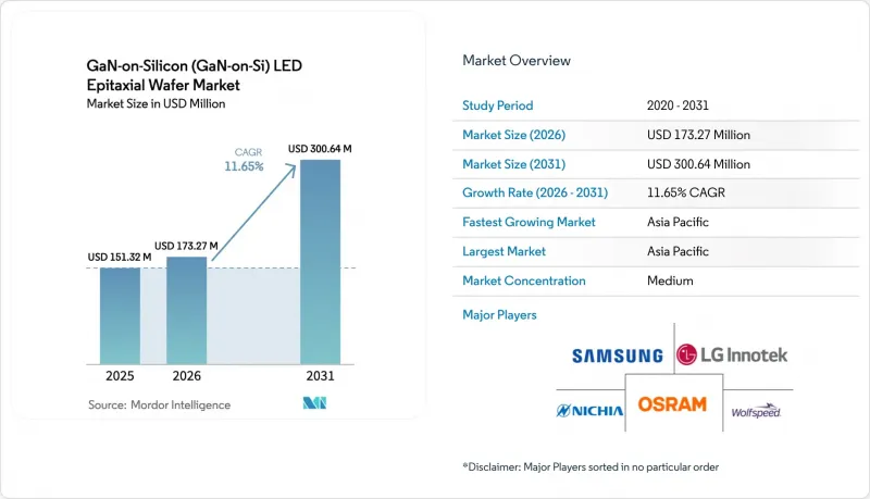
The GaN-on-Silicon LED epitaxial wafer market size is expected to increase from USD 0.151 billion in 2025 to USD 0.173 billion in 2026 and reach USD 0.301 billion by 2031, growing at a CAGR of 11.65% over 2026-2031.
Persistent regulatory pressure on lamp efficacy, the migration to 200 mm processing, and micro-LED adoption in augmented-reality (AR) devices are converging to widen the commercial appeal of GaN-on-Si epitaxy. Across lighting classes, LED penetration has already made incandescent and halogen formats economically obsolete, yet tightening standards in the United States, the European Union, China, and India are expanding the addressable market for more efficient die architectures. Foundries view the compatibility of silicon substrates with existing CMOS lines as a capital-saving lever, spurring vendors to pilot 300 mm MOCVD tools that can deliver nine times the die output of 100 mm sapphire runs. Momentum is reinforced by vertically integrated display programs targeting sub-10 µm pixels, where GaN-on-Si eliminates the wafer-to-driver bonding step that sapphire requires. Competitive dynamics remain moderate because roughly fifteen players control reactor capacity and hold the process know-how needed to keep defect densities within acceptable limits.
Global GaN-on-Silicon (GaN-on-Si) LED Epitaxial Wafer Market Trends and Insights
Increasing Demand for Energy-Efficient Solid-State Lighting
Solid-state lighting accounted for 65% of installed luminaires in 2025, yet the International Energy Agency calculated in 2026 that another 30% efficiency gain remains technically achievable, leaving ample headroom for the GaN-on-Silicon LED epitaxial wafer market to grow. The U.S. Department of Energy rule, effective July 2028, mandates lamp efficacies that cannot be met by incandescent or halogen technology, explicitly citing alternative substrate options, including silicon, as viable design pathways. Fixture makers addressing residential and commercial retrofits now face dual pressures to lower bill-of-materials cost and exceed 130 lm/W efficacy thresholds, and larger-diameter silicon wafers reduce per-lumen cost by up to 25% compared with 100 mm sapphire. Utility rebate programs in North America reinforce demand by linking incentives to high-efficacy product listings. Collectively, these forces sustain a multiyear pull for GaN-on-Si epitaxy across high-volume lighting classes.
Cost Reduction Potential of GaN-on-Si Substrates Versus Sapphire
Silicon substrates sell for USD 50-70 per 200 mm wafer, roughly one-eighth the price of comparable sapphire, creating a structural advantage that expands as diameters scale upward. Demonstrations in 2025 showed that 5.25 X 108 cm-2 dislocation densities are now routine, cutting the efficiency gap with sapphire while still preserving a 70% substrate-cost delta. In reactor economics, a 200 mm GaN-on-Si run produces four times the die area of a 100 mm sapphire load, enabling a single tool to support 500,000 onboard-charger LEDs yearly, according to a Shanghai materials supplier. Such scale profitability, however, hinges on maintaining yields above 85%, a target achievable only with real-time warp control and optimized buffer stacks. As these process refinements diffuse, silicon's price advantage is expected to offset residual efficiency penalties in cost-sensitive end markets.
High Dislocation Density and Yield Challenges in GaN-on-Si Epitaxy
The 17% lattice mismatch between silicon and gallium nitride drives threading dislocation densities near 1 X 109 cm-2, roughly two orders of magnitude higher than sapphire-based material and a primary cause of 10-15% lower external quantum efficiency. Buffer techniques such as 60-pair AlN/GaN multilayers can suppress stress but add up to USD 12 per wafer in extra reactor time. Warp above 100 µm on 200 mm substrates complicates lithography and dicing, forcing some fabs to scrap edge die, which undermines the cost benefits of larger wafers. Progress is uneven: while a handful of suppliers now report sub-30 µm bow metrics, the lack of standardized processes keeps average yields below the 90% benchmark enjoyed by sapphire competitors.
Other drivers and restraints analyzed in the detailed report include:
- Expansion of 200 mm and 300 mm CMOS Fabs for GaN-on-Si Epi
- Growth of Automotive LED Adoption for Headlamps and ADAS Sensors
- Competition from Sapphire-Based LED Wafers
For complete list of drivers and restraints, kindly check the Table Of Contents.
Segment Analysis
The 200 mm tier, representing the bridge between legacy 150 mm and emerging 300 mm production, is expanding faster than the overall GaN-on-Silicon LED epitaxial wafer market. In 2025 the 150 mm format still dominated shipments at 48.19%, thanks to its entrenched position in mid-power illumination and backlighting, yet equipment roadmaps now overwhelmingly favor larger diameters. Volume evaluations of 300 mm reactors in 2026 underscore a strategic pivot to 12-inch tools that yield ninefold more die than 100 mm sapphire lots, an arithmetic that resonates strongly with display panel makers. The GaN-on-Silicon LED epitaxial wafer market size advantage grows as wafer area increases, but only if edge exclusion and crack-related scrap remain minimal. Suppliers claiming sub-30 µm bow on 8-inch substrates report yields north of 90%, demonstrating that process control rather than raw diameter dictates economic viability.
Capital allocation is following the same logic. Foundries with depreciated 200 mm CMOS lines can retrofit chambers for GaN-on-Si at roughly 60% of the cost of new sapphire fabs, a figure that appeals to investors wary of cyclical LED margins. Although 100 mm and 150 mm wafers will persist in UV and prototyping roles, analysts expect new capacity additions after 2027 to skew heavily toward 200 mm and above. The inflection to 300 mm still confronts technical hurdles, most notably uniform gas flow and temperature gradients, but the payback, especially for high-pixel-count displays, is compelling enough that several tier-one equipment makers have committed to shipping production systems by 2027.
The GaN-On-Silicon (GaN-On-Si) LED Epitaxial Wafer Market Report is Segmented by Wafer Diameter (Up To 100 Mm, 150 Mm, 200 Mm, and 300 Mm and Above), Application (General Lighting, Automotive Lighting, Display and Backlighting, and Specialty and Industrial Lighting), and Geography. The Market Forecasts are Provided in Terms of Value (USD).
Geography Analysis
Asia-Pacific is both the manufacturing and innovation engine of the GaN-on-Silicon LED epitaxial wafer market. The region accounted for 66.93% of 2025 revenue, and national programs in China, Taiwan, and South Korea are forecast to drive a 12.64% CAGR through 2031. China alone has earmarked RMB 80 billion (USD 11.2 billion) for micro-LED infrastructure, much of which is dedicated to 200 mm and 300 mm GaN-on-Si fabs, ensuring local availability of large-diameter substrates. Taiwanese and Japanese vendors complement this scale with materials science expertise and equipment innovation. Nichia's mercury-free UV initiative and ROHM's decision to internalize GaN processes underscore a trend toward captive supply chains.
North America concentrates on high-value applications and policy-led adoption. The Department of Energy ruling that becomes enforceable in July 2028 virtually guarantees replacement of legacy incandescent stock, whereas partnerships such as onsemi-GlobalFoundries signal a willingness to incorporate GaN epitaxy into brownfield CMOS lines. European participation is anchored by Germany's Infineon, whose 300 mm wafer deliveries in Q4 2025 position the region as a node for automotive and industrial power devices. While South America, the Middle East, and Africa currently absorb only single-digit percentages of global shipments, off-grid solar lighting initiatives and industrial modernization efforts are likely to generate incremental demand for low-cost GaN-on-Si LEDs by the end of the decade.
Asia-Pacific's dominance is enhanced by vertical integration: Chinese and Taiwanese firms increasingly handle everything from raw GaN growth to finished LED modules, compressing the supply chain and accelerating time-to-market. Government subsidies lower risk for pilot lines, allowing experimentation with 300 mm formats that Western competitors regard as capital intensive. Nonetheless, intellectual-property enforcement challenges and export-control uncertainties temper the region's longer-term outlook, encouraging multinational OEMs to adopt dual-sourcing strategies that include North American or European epitaxial capacity.
- Nichia Corporation
- Wolfspeed Inc.
- Epistar Corporation
- OSRAM GmbH
- LG Innotek Co. Ltd.
- Samsung Electronics Co. Ltd.
- Plessey Semiconductors Ltd.
- Qorvo Inc.
- Infineon Technologies AG
- NXP Semiconductors N.V.
- Power Integrations Inc.
- Efficient Power Conversion Corporation
- Exagan SA
- STMicroelectronics N.V.
- Panasonic Corporation
- Toshiba Corporation
- ROHM Co. Ltd.
- Sumitomo Electric Industries Ltd.
- Sanan Optoelectronics Co. Ltd.
- Aixtron SE
- IQE plc
Additional Benefits:
- The market estimate (ME) sheet in Excel format
- 3 months of analyst support
TABLE OF CONTENTS
1 INTRODUCTION
- 1.1 Study Assumptions and Market Definition
- 1.2 Scope of the Study
2 RESEARCH METHODOLOGY
3 EXECUTIVE SUMMARY
4 MARKET LANDSCAPE
- 4.1 Market Overview
- 4.2 Market Drivers
- 4.2.1 Increasing Demand For Energy-Efficient Solid-State Lighting
- 4.2.2 Cost Reduction Potential Of GaN-on-Si Substrates Versus Sapphire
- 4.2.3 Government Regulations Phasing-Out Incandescent And Halogen Bulbs
- 4.2.4 Growth Of Automotive LED Adoption For Headlamps And ADAS Sensors
- 4.2.5 Integration Of GaN-Based Micro-LED Arrays For AR Displays
- 4.2.6 Expansion Of 200 mm And 300 mm CMOS Fabs For GaN-on-Si Epi
- 4.3 Market Restraints
- 4.3.1 High Dislocation Density And Yield Challenges In GaN-on-Si Epitaxy
- 4.3.2 Competition From Sapphire-Based LED Wafers
- 4.3.3 Limited Availability Of Patterned Si Substrates With Stress Control
- 4.3.4 Risk Of IP Litigation In GaN Epitaxy Processes
- 4.4 Industry Analysis
- 4.5 Impact Of Macroeconomic Factors On The Market
- 4.6 Porter's Five Forces Analysis
- 4.6.1 Bargaining Power Of Suppliers
- 4.6.2 Bargaining Power Of Buyers
- 4.6.3 Threat Of New Entrants
- 4.6.4 Threat Of Substitutes
- 4.6.5 Intensity Of Competitive Rivalry
5 MARKET SIZE AND GROWTH FORECASTS (VALUE)
- 5.1 By Wafer Diameter
- 5.1.1 Upto 100 mm
- 5.1.2 150 mm
- 5.1.3 200 mm
- 5.1.4 300 mm and Above
- 5.2 By Application
- 5.2.1 General Lighting
- 5.2.2 Automotive Lighting
- 5.2.3 Display and Backlighting
- 5.2.4 Specialty and Industrial Lighting
- 5.3 By Geography
- 5.3.1 North America
- 5.3.2 Europe
- 5.3.3 Asia-Pacific
- 5.3.4 Rest of the World
6 COMPETITIVE LANDSCAPE
- 6.1 Market Concentration
- 6.2 Strategic Moves
- 6.3 Market Share Analysis
- 6.4 Company Profiles (includes Global Level Overview, Market Level Overview, Core Segments, Financials as available, Strategic Information, Market Rank/Share, Products and Services, Recent Developments)
- 6.4.1 Nichia Corporation
- 6.4.2 Wolfspeed Inc.
- 6.4.3 Epistar Corporation
- 6.4.4 OSRAM GmbH
- 6.4.5 LG Innotek Co. Ltd.
- 6.4.6 Samsung Electronics Co. Ltd.
- 6.4.7 Plessey Semiconductors Ltd.
- 6.4.8 Qorvo Inc.
- 6.4.9 Infineon Technologies AG
- 6.4.10 NXP Semiconductors N.V.
- 6.4.11 Power Integrations Inc.
- 6.4.12 Efficient Power Conversion Corporation
- 6.4.13 Exagan SA
- 6.4.14 STMicroelectronics N.V.
- 6.4.15 Panasonic Corporation
- 6.4.16 Toshiba Corporation
- 6.4.17 ROHM Co. Ltd.
- 6.4.18 Sumitomo Electric Industries Ltd.
- 6.4.19 Sanan Optoelectronics Co. Ltd.
- 6.4.20 Aixtron SE
- 6.4.21 IQE plc
7 MARKET OPPORTUNITIES AND FUTURE OUTLOOK
- 7.1 White-Space and Unmet-Need Assessment

