PUBLISHER: Mordor Intelligence | PRODUCT CODE: 2063427

PUBLISHER: Mordor Intelligence | PRODUCT CODE: 2063427
Micro LED Chip Mass Transfer Equipment - Market Share Analysis, Industry Trends & Statistics, Growth Forecasts (2026 - 2031)
According to Mordor Intelligence, the micro lED chip mass transfer equipment market size is projected to expand from USD 281.65 billion in 2025 and USD 318.49 billion in 2026 to USD 550.49 billion by 2031, registering a CAGR of 11.57% between 2026 to 2031.
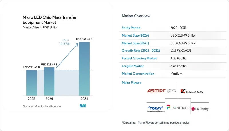
This report is Segmented by Transfer Technology (Elastomer Stamp Transfer, Laser Transfer, Electrostatic Transfer, Fluidic Transfer, and More), Equipment Architecture (Wafer-To-Wafer, Wafer-To-Panel, Chip-To-Panel, and More), Application (Consumer Electronics, AR/VR Displays, and More), and Geography. The Market Forecasts are Provided in Terms of Value (USD).
Global Micro LED Chip Mass Transfer Equipment Market Trends and Insights
Growing Demand for Micro LED Displays in Premium Consumer Electronics
MicroLED is now the de facto successor to OLED in flagship smartphones, watches, and large-screen televisions. Samsung expanded its Micro RGB television line in 2026 to 55-115-inch sizes, normalizing millions of microLED dies per panel and boosting annual tool utilization at key outsourced assembly partners. PlayNitride, working with AUO, scaled six-inch GaN-on-silicon wafer output for smartwatch and automotive orders, driving a 20% boost in capacity plans for 2026. Display makers are accelerating the shift from blue-chip plus quantum-dot color conversion to true RGB transfer, which demands three sequential placement cycles but increases luminous efficiency by up to 40%. LG Display demonstrated a 22.3-inch active-matrix microLED tile in 2024 that stitches into 136-inch 4K walls, a modular strategy that relies on sub-50 micrometer stamp transfer at commercial throughputs. Research firm Omdia expects microLED display revenue to double between 2025 and 2026, confirming the near-term uptick in equipment orders omdia.tech.informa.com.
Ongoing Investments in Next-Gen Display Manufacturing Lines
Asia-Pacific panel makers are repurposing legacy LTPS and a-Si fabs for microLED pilot lines, funneling more than USD 1 billion between 2024 and 2025 into wafer-to-panel and hybrid tools. BOE's sixth-generation line in Chongqing entered production in early 2025, with 50,000 sheets per month supporting both LTPO backplanes and a separate microLED pilot zone. Tianma completed a RMB 1.1 billion (USD 155 million) plant in December 2024 featuring a G3.5 full-laser transfer system rated at 40 million chips per hour. AUO's 4.5-generation campus reached mass production in 2025, supplying Sony Mobility with cockpit modules for the 2026 AFEELA launch. HC SemiTek's Zhuhai epi-wafer line, live since November 2024, reduces China's import dependency and enhances wafer availability for downstream transfer qualification. While the bulk of spending centers on China, Taiwan, and South Korea, U.S. firms leverage CHIPS Act credits to co-locate pilot lines with advanced-packaging hubs.
High Capital Expenditure and Process Complexity vs. OLED Alternatives
A greenfield microLED line requires USD 200-300 million, roughly double the incremental cost of extending OLED evaporation and encapsulation capacity. LG Display's W 1 trillion (USD 750 million) budget for 2025-2027 earmarks a majority for OLED, keeping microLED in pilot modules that piggyback on AMOLED backplanes lgdisplay.com. AUO's 4.5-generation plant cost NTD 2 billion (USD 66.7 million) yet supports only 10,000 six-inch wafers per month, illustrating the constrained economies of scale auo.com. MicroLED production involves up to twelve process steps, each compounding yield loss to roughly 60-70% at early maturity, compared with OLED's 85-90% onlinelibrary.wiley.com. Samsung mitigates the burden by segmenting its product line: ultra-luxury 110-140 inch self-emissive walls absorb higher costs, whereas cost-optimized Micro RGB televisions trade off per-pixel control for attainable price points news.samsung.com. Equipment builders respond with modular tools that allow staged investments, but this elongates payback to six-eight years for conservative panel makers.
Other drivers and restraints analyzed in the detailed report include:
- Advancements in Mass-Transfer Throughput and Yield Metrics
- Government Incentives for Domestic Semiconductor-Equipment Production
- Limited Supply Chain for High-Uniformity MicroLED Epitaxial Wafers
For complete list of drivers and restraints, kindly check the Table Of Contents.
Segment Analysis
Elastomer-stamp tools dominated 2025 with 41.68% of the Micro LED chip mass transfer equipment market size, leveraging decades of printed-electronics know-how to place 10-20 micrometer dies across large signage substrates at 10,000-20,000 dies per second. Their simplicity, low consumable cost, and compatibility with curved automotive clusters sustain demand. Yet applications that push below 5 micrometers, such as retinal-resolution AR optics, expose stamp-induced edge damage and adhesion drift. Laser-assisted forward transfer therefore captured almost one-third of revenue, propelled by Coherent's UVtransfer and similar excimer solutions that hit sub-micrometer tolerances at tenfold higher speeds. Fluidic and electrostatic approaches remain niche, but they seed patents that incumbents cannot ignore.
Hybrid designs marry the raw speed of laser release with the gentle landing control of electrostatic or vacuum pick-and-place, enabling a single frame to process die ranges from 3 to 100 micrometers. The combination lowers cycle time by roughly 40% compared with sequential tools and underpins the 12.33% CAGR expected for hybrid platforms. VueReal's cartridge system, capable of swapping pre-filled die cassettes between builds, epitomizes high-mix agility. Meanwhile, ASMPT integrates auto-repair heads that rework sub-0.01% mismatches in-situ, an essential feature once panel die counts exceed 20 million. The performance blend positions hybrid systems as default selections for new fabs that must hedge against die-size evolution over the planning horizon.
Geography Analysis
Asia-Pacific dominated with 62.83% of Micro LED chip mass transfer equipment market revenue in 2025, anchored by Chinese and Taiwanese conglomerates that co-locate epi-growth, transfer, and backplane assembly within cluster campuses. Tianma, BOE, and Visionox collectively deployed more than USD 1.5 billion on pilot and Gen 4.5 lines between 2024 and 2025, compressing development loops and giving regional vendors first-mover runway. South Korea's KRW 484 billion (USD 350 million) incentive blueprint adds strategic depth by plugging domestic wafer and bonding gaps, a move likely to lift local tool purchases once qualification milestones are met.
North America, forecast to expand at a 12.16% CAGR, is translating CHIPS Act tax credits and grants into green-field investments that span epi-growth through heterogeneous integration. Early awards cover Amkor, GlobalFoundries, Intel, and SK Hynix advanced-packaging hubs that can repurpose laser-transfer platforms for chiplets and microLEDs alike. Meta's Haylo fab in New York State anchors the supply chain for sub-5 micrometer blue and green dies, while Veeco's Lumina+ MOCVD shipments to Rocket Lab illustrate upstream-downstream pull effects that ripple into mass-transfer demand.
Europe, at roughly 8% share, lacks high-volume display makers yet benefits from EU Chips Act depreciation perks that spur R&D labs and pilot modules aimed at automotive interiors and aerospace HUDs. Rest-of-World regions, mainly Southeast Asia and the Middle East, remain niche assembly hubs that hedge geopolitical risk for Chinese and Taiwanese brands but have not yet placed substantial tool orders.
- ASMPT Ltd.
- Kulicke & Soffa Industries Inc.
- Toray Engineering Co. Ltd.
- PlayNitride Inc.
- LG Display Co. Ltd.
- K&S NeoLight (Rohinni-K&S JV)
- Rohinni LLC
- TDK Corporation
- Coherent Corp.
- Aixtron SE
- Veeco Instruments Inc.
- QMAT Inc.
- Samsung Electronics Co. Ltd.
- BOE Technology Group Co. Ltd.
- Visionox Technology Inc.
- AUO Corporation
- Innolux Corporation
- Saphlux Inc.
- Plessey Semiconductors Ltd.
- Tianma Microelectronics Co. Ltd.
Additional Benefits:
- The market estimate (ME) sheet in Excel format
- 3 months of analyst support
TABLE OF CONTENTS
1 INTRODUCTION
- 1.1 Study Assumptions and Market Definition
- 1.2 Scope of the Study
2 RESEARCH METHODOLOGY
3 EXECUTIVE SUMMARY
4 MARKET LANDSCAPE
- 4.1 Market Overview
- 4.2 Market Drivers
- 4.2.1 Growing Demand For Micro LED Displays In Premium Consumer Electronics
- 4.2.2 Ongoing Investments In Next-Gen Display Manufacturing Lines
- 4.2.3 Advancements In Mass Transfer Throughput And Yield Metrics
- 4.2.4 Government Incentives For Domestic Semiconductor Equipment Production
- 4.2.5 Adoption Of Chiplet-Ready Transfer Platforms For Modular AR/VR Optics
- 4.2.6 Integration Of AI-Based Vision Systems For In-Process Defect Detection
- 4.3 Market Restraints
- 4.3.1 High Capital Expenditure And Process Complexity Vs. OLED Alternatives
- 4.3.2 Limited Supply Chain For High-Uniformity Micro LED Epitaxial Wafers
- 4.3.3 Thermal Stress-Induced Warpage During Wafer-to-Panel Transfer Cycles
- 4.3.4 IP Litigation Risks Around Elastomer Stamp Patents In China
- 4.4 Industry Supply-Chain Analysis
- 4.5 Regulatory Landscape
- 4.6 Impact of Macroeconomic Factors
- 4.7 Porter's Five Forces Analysis
- 4.7.1 Bargaining Power of Suppliers
- 4.7.2 Bargaining Power of Buyers
- 4.7.3 Threat of New Entrants
- 4.7.4 Threat of Substitutes
- 4.7.5 Intensity of Competitive Rivalry
5 MARKET SIZE AND GROWTH FORECASTS (VALUE)
- 5.1 By Transfer Technology
- 5.1.1 Elastomer Stamp Transfer
- 5.1.2 Laser Transfer
- 5.1.3 Electrostatic Transfer
- 5.1.4 Fluidic Transfer
- 5.1.5 Hybrid Transfer
- 5.2 By Equipment Architecture
- 5.2.1 Wafer-to-Wafer
- 5.2.2 Wafer-to-Panel
- 5.2.3 Chip-to-Panel
- 5.2.4 Repair Transfer Systems
- 5.3 By Application
- 5.3.1 Consumer Electronics
- 5.3.2 AR/VR Displays
- 5.3.3 Automotive Displays
- 5.3.4 Commercial Displays
- 5.4 By Geography
- 5.4.1 Asia-Pacific
- 5.4.2 North America
- 5.4.3 Europe
- 5.4.4 Rest of World
6 COMPETITIVE LANDSCAPE
- 6.1 Market Concentration
- 6.2 Strategic Moves
- 6.3 Market Share Analysis
- 6.4 Company Profiles (includes Global Level Overview, Market Level Overview, Core Segments, Financials as available, Strategic Information, Market Rank/Share, Products and Services, Recent Developments)
- 6.4.1 ASMPT Ltd.
- 6.4.2 Kulicke & Soffa Industries Inc.
- 6.4.3 Toray Engineering Co. Ltd.
- 6.4.4 PlayNitride Inc.
- 6.4.5 LG Display Co. Ltd.
- 6.4.6 K&S NeoLight (Rohinni-K&S JV)
- 6.4.7 Rohinni LLC
- 6.4.8 TDK Corporation
- 6.4.9 Coherent Corp.
- 6.4.10 Aixtron SE
- 6.4.11 Veeco Instruments Inc.
- 6.4.12 QMAT Inc.
- 6.4.13 Samsung Electronics Co. Ltd.
- 6.4.14 BOE Technology Group Co. Ltd.
- 6.4.15 Visionox Technology Inc.
- 6.4.16 AUO Corporation
- 6.4.17 Innolux Corporation
- 6.4.18 Saphlux Inc.
- 6.4.19 Plessey Semiconductors Ltd.
- 6.4.20 Tianma Microelectronics Co. Ltd.
7 MARKET OPPORTUNITIES AND FUTURE OUTLOOK
- 7.1 White-Space and Unmet-Need Assessment

