PUBLISHER: Mordor Intelligence | PRODUCT CODE: 2063669

PUBLISHER: Mordor Intelligence | PRODUCT CODE: 2063669
Micro LED Chips - Market Share Analysis, Industry Trends & Statistics, Growth Forecasts (2026 - 2031)
According to Mordor Intelligence, the micro LED chips market size is projected to expand from USD 0.108 billion in 2025 and USD 0.137 billion in 2026 to USD 2.71 billion by 2031, registering a CAGR of 81.77% between 2026 and 2031.
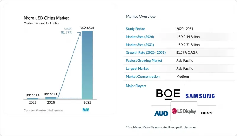
This report is Segmented by Chip Size (1-20 Mm, 20-50 Mm, and More), Semiconductor Material (GaN/InGaN and AlGaInP), Application (Smartwatches and Wearables, AR/VR Near-Eye Displays, Television, Smartphones and Tablets, Automotive Displays, Digital Signage/Large Displays, and More), and Geography (North America, Europe, Asia Pacific, and More). The Market Forecasts are Provided in Terms of Value (USD).
Global Micro LED Chips Market Trends and Insights
Accelerating Apple and Samsung In-house Micro LED Integration Roadmaps
CES 2026 confirmed that Samsung's television roadmap now spans 55-130-inch Micro RGB models, achieving 100% BT.2020 color without blue-light hazard certification. LG countered with its Micro RGB Evo series, signaling a strategic pivot away from reliance on OLEDs and toward vertically integrated supply chains. Sony trademarked "True RGB" for its Crystal LED S Series, underscoring that premium brands see branding as a lever to capture early adopters. Apple remains publicly silent, but its watch prototypes suggest an exploratory posture that contrasts with Samsung's aggressive scale-up. This divergence creates a two-speed ecosystem where television economics may subsidize die-size learning curves for wearable and AR form factors.
Cost Declines from Six-Inch GaN-on-Si Wafer Scale-Up
BOE HC Semitek's USD 700 million Zhuhai project will deliver 58,000 six-inch wafers annually, quadrupling usable die area relative to legacy four-inch lines and slashing per-chip epitaxial cost by roughly 50%. PlayNitride projects that the learning curve will push the micro LED chip market to market size parity with OLED by 2028 for high-brightness use cases. Hunan University's six-inch GaN-on-Si wafers exceeding 10 million nits confirm optical integrity at larger diameters. A USD 1.5 billion CHIPS Act award is enabling GlobalFoundries to build a Western Hemisphere GaN-on-Si source, reducing geopolitical risk for automotive and defense applications. Together, these moves compress the cost gap with OLED and reposition supply chains geographically.
Yield < 60% for Sub-10 µm Red LEDs Below 4-Inch Wafers
The external quantum efficiency of sub-10 µm AlGaInP red dies rose to 22.3% with aluminum-nitride passivation, yet commercial yields still trail those of green and blue counterparts by a wide margin. Side-wall oxidation reduces non-radiative recombination but has not lifted yields above 60%, creating scrap costs that erode margins. Samsung and LG navigate this by using larger red dies for televisions, where die counts per panel are lower. Wearable and AR devices instead deploy blue GaN arrays with quantum-dot down-conversion, adding cost and process steps. Industry consensus holds that six-inch AlGaInP wafers could reduce edge exclusion and thermal gradients, but no public yield data yet exist for that diameter.
Other drivers and restraints analyzed in the detailed report include:
- Laser-Based Mass-Transfer Throughput Gains > 400 Chips/Sec
- Automotive OEM Demand for Sun-Readable HUDs in EV Platforms
- > USD 600 M CapEx Barrier for Greenfield High-Volume Lines
For complete list of drivers and restraints, kindly check the Table Of Contents.
Segment Analysis
The 1-20 µm segment is forecast to post an 83.21% CAGR, the fastest among all size classes, as Garmin's USD 1,999.99 Fenix 8 Pro MicroLED proves consumer readiness to pay for 4,500-nit daylight performance. Jade Bird Display's 10,160 PPI Roadrunner micro panel showcases that density, not die cost, defines near-eye adoption curves. However, battery life still trails AMOLED, and driver IC integration must improve to close the power gap.
Large-format displays gravitate toward 50-100 µm dies, where yields are higher, and mass-transfer tolerances are looser. Samsung's 130-inch set and LG's 100-inch model rely on sub-100 µm RGB LEDs to hit 100% BT.2020 color while maintaining cost discipline at wall-scale diagonals. Automotive HUD units sit between, using 20-50 µm dies to balance density with throughput; BOE's HERO 2.0 and Tianma's modules exemplify this sweet spot.
Geography Analysis
Asia Pacific generated 62.30% of 2025 revenue and is projected to grow at an 84.36% CAGR, making it the anchor of the micro LED chips market. China's "speed-and-scale" model is epitomized by BOE's 58,000-wafer Zhuhai fab and San'an's 5,000 kk-unit mini-LED ramp, giving the region unmatched die supply depth. Taiwan champions ultra-high-resolution niches; AUO's Garmin panel win, and ASE's USD 579 million backend plant in Kaohsiung reflect an ecosystem strategy. South Korea leads in integrated TV assembly but still imports many chips, indicating room for upstream investment.
North America's outlook hinges on the execution of the CHIPS Act. USD 1.5 billion is funding GlobalFoundries' GaN-on-Si line, while Intel and TSMC are collecting a combined USD 25.5 billion for advanced-node fabs that may house micro LED and driver components. A 25% tariff on imported advanced chips, effective January 2026, could nudge OEMs toward domestic sourcing but raises near-term costs. Europe lacks comparable incentives, relying on imports for epitaxy and panels, though automotive OEM interest via Peugeot indicates latent demand.
South America and the Middle East are early-stage markets where premium outdoor signage and automotive upgrades will seed adoption. Local manufacturing is absent, but micro LEDs' longevity and brightness can justify imports for flagship retail facades and luxury EV dashboards. Regulatory gaps, especially around automotive safety standards, are global, slowing deployment even where technical readiness is proven.
- Samsung Electronics Co., Ltd.
- LG Display Co., Ltd.
- Sony Group Corporation
- AUO Corporation
- PlayNitride Inc.
- Epistar Corporation
- Jade Bird Display Inc.
- Plessey Semiconductors Ltd.
- Aledia S.A.
- VueReal Inc.
- San'an Optoelectronics Co., Ltd.
- Innolux Corporation
- Leyard Optoelectronic Co., Ltd.
- Unilumin Group Co., Ltd.
- Kyocera Corporation
- Cree LED, a Smart Global Holdings Company
- OSRAM Opto Semiconductors GmbH
Additional Benefits:
- The market estimate (ME) sheet in Excel format
- 3 months of analyst support
TABLE OF CONTENTS
1 INTRODUCTION
- 1.1 Study Assumptions and Market Definition
- 1.2 Scope of the Study
2 RESEARCH METHODOLOGY
3 EXECUTIVE SUMMARY
4 MARKET LANDSCAPE
- 4.1 Market Overview
- 4.2 Market Drivers
- 4.2.1 Accelerating Apple and Samsung In-house Micro LED Integration Roadmaps
- 4.2.2 Cost Declines from Six-Inch GaN-on-Si Wafer Scale-Up
- 4.2.3 Laser-Based Mass-Transfer Throughput Gains >400 Chips/Sec
- 4.2.4 Automotive OEM Demand for Sun-Readable HUDs in EV Platforms
- 4.2.5 Government CHIPS-style Incentives for Domestic Micro-Display Fabs
- 4.2.6 Quantum-Dot Color Conversion Surpassing 80 % Efficiency
- 4.3 Market Restraints
- 4.3.1 Yield <60 % for Sub-10 µm Red LEDs Below 4-inch Wafers
- 4.3.2 >USD 600 M CapEx Barrier for Greenfield High-Volume Lines
- 4.3.3 Lack of Automotive Qualification Standards for Micro LED HUDs
- 4.3.4 Concentrated Supply of GaN-on-Si Wafers in East Asia
- 4.4 Industry Supply-Chain Analysis
- 4.5 Impact of Macroeconomic Factors on the Market
- 4.6 Regulatory Landscape
- 4.7 Technological Outlook
- 4.8 Porter's Five Forces Analysis
- 4.8.1 Threat of New Entrants
- 4.8.2 Bargaining Power of Suppliers
- 4.8.3 Bargaining Power of Buyers
- 4.8.4 Threat of Substitutes
- 4.8.5 Competitive Rivalry
5 MARKET SIZE AND GROWTH FORECASTS (VALUE)
- 5.1 By Chip Size
- 5.1.1 1-20 µm
- 5.1.2 20-50 µm
- 5.1.3 50-100 µm
- 5.2 By Semiconductor Material
- 5.2.1 GaN / InGaN
- 5.2.2 AlGaInP
- 5.3 By Application
- 5.3.1 Smartwatches & Wearables
- 5.3.2 AR/VR Near-Eye Displays
- 5.3.3 Television
- 5.3.4 Smartphones & Tablets
- 5.3.5 Automotive Displays
- 5.3.6 Digital Signage / Large Displays
- 5.3.7 Other Applications (Industrial, Medical)
- 5.4 By Geography
- 5.4.1 North America
- 5.4.2 Europe
- 5.4.3 Asia Pacific
- 5.4.4 South America
- 5.4.5 Middle East and Africa
6 COMPETITIVE LANDSCAPE
- 6.1 Market Concentration
- 6.2 Strategic Moves
- 6.3 Market Share Analysis
- 6.4 Company Profiles (includes Global Level Overview, Market Level Overview, Core Segments, Financials as available, Strategic Information, Market Rank/Share, Products and Services, Recent Developments)
- 6.4.1 Samsung Electronics Co., Ltd.
- 6.4.2 LG Display Co., Ltd.
- 6.4.3 Sony Group Corporation
- 6.4.4 AUO Corporation
- 6.4.5 PlayNitride Inc.
- 6.4.6 Epistar Corporation
- 6.4.7 Jade Bird Display Inc.
- 6.4.8 Plessey Semiconductors Ltd.
- 6.4.9 Aledia S.A.
- 6.4.10 VueReal Inc.
- 6.4.11 San'an Optoelectronics Co., Ltd.
- 6.4.12 Innolux Corporation
- 6.4.13 Leyard Optoelectronic Co., Ltd.
- 6.4.14 Unilumin Group Co., Ltd.
- 6.4.15 Kyocera Corporation
- 6.4.16 Cree LED, a Smart Global Holdings Company
- 6.4.17 OSRAM Opto Semiconductors GmbH
7 MARKET OPPORTUNITIES AND FUTURE OUTLOOK
- 7.1 White-Space and Unmet-Need Assessment

