PUBLISHER: Mordor Intelligence | PRODUCT CODE: 2044007

PUBLISHER: Mordor Intelligence | PRODUCT CODE: 2044007
Prime Polished Wafer - Market Share Analysis, Industry Trends & Statistics, Growth Forecasts (2026 - 2031)
The prime polished wafer market size is projected to be 8.86 billion square inches in 2025, 9.26 billion square inches in 2026, and reach 11.76 billion square inches by 2031, growing at a CAGR of 4.88% from 2026 to 2031.
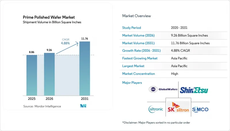
Semiconductor manufacturers are reallocating capital toward advanced logic nodes, automotive electrification, and high-bandwidth memory, all of which consume wafer surface area far more rapidly than traditional consumer-electronics refresh cycles. Foundries' shift to sub-3 nm process technology, coupled with the ramp-up of through-silicon-via packaging, is concentrating demand in the 300 mm diameter class that already dominates the prime polished wafer market. Asia-Pacific's contract manufacturing base keeps the region in a leadership position, while the United States and Europe are using incentive packages to on-shore strategic capacity despite the resulting cost penalties. Suppliers remain cautious on new crystal-growth investments because each 300 mm high-purity ingot line ranges from USD 2 million to USD 5 million and can take two years to qualify.
Global Prime Polished Wafer Market Trends and Insights
Rising EV Penetration and Shift Toward 800-V Vehicle Platforms
Electric vehicles adopting 800-volt architectures require silicon-carbide traction inverters that consume far larger prime polished wafer volumes per car than silicon devices. Wolfspeed's commercial 200 mm SiC launch in September 2025 increases chips-per-wafer by roughly 85%, yet supply is still bottlenecked by 7- to 14-day crystal-growth cycles. Multiple major automakers already qualify SiC MOSFETs rated up to 1,200 V, pushing demand firmly upward.
Rapid Build-Out of 800-V Charging Infrastructure
Europe and China are adding thousands of 150- to 350-kW charging stalls that embed SiC modules for rectification and power-factor correction. Each ultra-fast charger needs multiple 200 mm wafers, creating a second-order pull on the prime polished wafer market. Subsidies accelerate installation schedules, compressing suppliers' ability to add new boule capacity.
Limited Availability of 200 mm Substrates
200 mm SiC boules require long growth times and specialized furnaces. Substrate lead times stretch beyond 40 weeks for smaller customers as automotive OEMs lock in multi-year contracts, leaving the rest of the prime polished wafer market scrambling for allocation.
Other drivers and restraints analyzed in the detailed report include:
- High-Temperature, High-Frequency Performance Advantages Over Si
- Government Incentives for Wide-Band-Gap Fabs
- Packaging-Induced Thermo-Mechanical Stress
For complete list of drivers and restraints, kindly check the Table Of Contents.
Segment Analysis
The 300 mm class accounted for 73.39% of prime polished wafer market share in 2025 and is forecast to grow at a 5.55% CAGR through 2031. TSMC's USD 56 billion capital plan for 2026, of which 70-80% goes to sub-3 nm logic, underscores the relentless shift toward large-diameter processing. The prime polished wafer market size for this diameter will continue expanding as high-bandwidth memory and AI accelerators require four-to-eight times more wafer area per server than conventional workloads. Intel's USD 165 billion Arizona "gigafab" cluster and GlobalWafers' Texas line add regional redundancy, satisfying domestic-content rules while creating new logistic hubs.
The 200 mm segment remains essential for analog, mixed-signal, and power devices, particularly SiC MOSFETs where the economics still favor smaller diameters. Okmetic's Finnish expansion and Wolfspeed's 200 mm SiC wafers show the dual-track strategy of suppliers addressing both mainstream silicon and specialty needs. Up-to-150 mm formats are declining, yet they persist in legacy automotive microcontrollers and RF GaAs devices. As crystal-growth breakthroughs reduce defect densities, 200 mm SiC supply could loosen post-2028, but near-term scarcity keeps prices elevated and reinforces multi-sourcing behavior among fabs.
The Prime Polished Wafer Market Report is Segmented by Wafer Diameter (Up To 150 Mm, 200 Mm, 300 Mm), Semiconductor Device Type (Logic, Memory, Analog, Discrete, Other), End-User (Consumer Electronics, Industrial, Telecommunications, Automotive, Other), and Geography (North America, Europe, Asia-Pacific, South America, Middle East and Africa). Market Forecasts are Provided in Terms of Volume (Square Inches).
Geography Analysis
Asia-Pacific shipped 81.39% of global prime polished wafer volumes in 2025 and is set to grow at 5.21% CAGR through 2031. Regional giants such as TSMC, Samsung, and SK Siltron continue expanding deeply integrated clusters that bundle front-end, packaging, and testing. China's SMIC added 40 k 12-inch-equivalent wafers per month in 2026, achieving 95.7% utilization despite tool export controls. Subsidies under China's USD 47.5 billion IC Fund Phase III buttress domestic SiC supply chains.
North America is reversing decades of offshoring by tapping USD 39 billion in CHIPS incentives. GlobalWafers' USD 3.5 billion Texas plant, Intel's Arizona gigafab, and Wolfspeed's SiC mega-facility collectively drive a region-wide surge in demand for prime polished wafers. Mexico's ascending role in assembly and test adds downstream pull.
Europe remains fab-constrained for leading-edge logic yet excels in strategic materials. STMicroelectronics secured EUR 2.9 billion (USD 3.2 billion) to scale SiC in Italy, and discussions continue on a potential TSMC-run Dresden fab that would localize 300 mm automotive capacity. Soitec and Siltronic provide regionally anchored SOI and high-flatness substrates, keeping Europe relevant in the prime polished wafer market value chain. Emerging investments across South America and the Middle East and Africa favor mature-node fabs servicing automotive and industrial customers close to end markets.
- Shin-Etsu Handotai Co., Ltd.
- SUMCO Corporation
- GlobalWafers Co., Ltd.
- Siltronic AG
- SK Siltron Co., Ltd.
- Soitec SA
- Okmetic Oyj
- Wafer Works Corporation
- Ferrotec Holdings Corporation
- Hangzhou Crystal Silicon Technology Co., Ltd.
- Poshing Electronics Co., Ltd.
- MiCo Co., Ltd.
- Tokuyama Corporation
- Topsil Semiconductor Materials A/S
- GCL Technology Holdings Limited
- Zhejiang Jingsheng Mechanical & Electrical Co., Ltd.
- II-VI Incorporated
- AEPI Group (Sil'Tronix Silicon Technologies)
- Advantest Corporation
- Shanghai SIM-AXIS Semiconductor Materials Co., Ltd.
Additional Benefits:
- The market estimate (ME) sheet in Excel format
- 3 months of analyst support
TABLE OF CONTENTS
1 INTRODUCTION
- 1.1 Study Assumptions and Market Definition
- 1.2 Scope of the Study
2 RESEARCH METHODOLOGY
3 EXECUTIVE SUMMARY
4 MARKET LANDSCAPE
- 4.1 Market Overview
- 4.2 Industry Value-Chain Analysis
- 4.3 Regulatory Landscape
- 4.4 Impact of Macroeconomic Factors
- 4.5 Technology Analysis
- 4.6 Regulatory Outlook
- 4.7 Porter's Five Forces Analysis
- 4.7.1 Bargaining Power of Suppliers
- 4.7.2 Bargaining Power of Buyers
- 4.7.3 Threat of New Entrants
- 4.7.4 Threat of Substitutes
- 4.7.5 Intensity of Competitive Rivalry
- 4.8 Market Drivers
- 4.8.1 Rising EV Penetration and Shift Toward 800-V Vehicle Platforms
- 4.8.2 Rapid Build-Out of 800-V Charging Infrastructure
- 4.8.3 High-Temperature, High-Frequency Performance Advantages Over Si
- 4.8.4 Government Incentives for Wide-Band-Gap Fabs
- 4.8.5 Emergence of Vertically-Integrated SiC Supply Chains in China
- 4.8.6 Novel 200 mm Bulk-Growth Breakthroughs Lowering Defect Density
- 4.9 Market Restraints
- 4.9.1 Limited Availability of 200 mm Substrates
- 4.9.2 Packaging-Induced Thermo-Mechanical Stress
- 4.9.3 Capital-Intensive Crystal-Growth Equipment
- 4.9.4 Recycling Challenges for SiC Kerf Waste
5 MARKET SIZE AND GROWTH FORECASTS (VOLUME)
- 5.1 By Wafer Diameter
- 5.1.1 Up to 150 mm
- 5.1.2 200 mm
- 5.1.3 300 mm
- 5.2 By Semiconductor Device Type
- 5.2.1 Logic
- 5.2.2 Memory
- 5.2.3 Analog
- 5.2.4 Discrete
- 5.2.5 Other Semiconductor Device Types (Optoelectronics, Sensors, Micro)
- 5.3 By End-User
- 5.3.1 Consumer Electronics
- 5.3.1.1 Mobile and Smartphones
- 5.3.1.2 PCs and Servers
- 5.3.2 Industrial
- 5.3.3 Telecommunications
- 5.3.4 Automotive
- 5.3.5 Other End-User Applications
- 5.3.1 Consumer Electronics
- 5.4 By Geography
- 5.4.1 North America
- 5.4.1.1 United States
- 5.4.1.2 Canada
- 5.4.1.3 Mexico
- 5.4.2 Europe
- 5.4.2.1 Germany
- 5.4.2.2 United Kingdom
- 5.4.2.3 France
- 5.4.2.4 Rest of Europe
- 5.4.3 Asia-Pacific
- 5.4.3.1 China
- 5.4.3.2 Japan
- 5.4.3.3 India
- 5.4.3.4 South Korea
- 5.4.3.5 Taiwan
- 5.4.3.6 Rest of Asia-Pacific
- 5.4.4 South America
- 5.4.5 Middle East
- 5.4.6 Africa
- 5.4.1 North America
6 COMPETITIVE LANDSCAPE
- 6.1 Market Concentration
- 6.2 Strategic Moves
- 6.3 Market Share Analysis
- 6.4 Company Profiles (includes Global Level Overview, Market Level Overview, Core Segments, Financials as available, Strategic Information, Market Rank/Share, Products and Services, Recent Developments)
- 6.4.1 Shin-Etsu Handotai Co., Ltd.
- 6.4.2 SUMCO Corporation
- 6.4.3 GlobalWafers Co., Ltd.
- 6.4.4 Siltronic AG
- 6.4.5 SK Siltron Co., Ltd.
- 6.4.6 Soitec SA
- 6.4.7 Okmetic Oyj
- 6.4.8 Wafer Works Corporation
- 6.4.9 Ferrotec Holdings Corporation
- 6.4.10 Hangzhou Crystal Silicon Technology Co., Ltd.
- 6.4.11 Poshing Electronics Co., Ltd.
- 6.4.12 MiCo Co., Ltd.
- 6.4.13 Tokuyama Corporation
- 6.4.14 Topsil Semiconductor Materials A/S
- 6.4.15 GCL Technology Holdings Limited
- 6.4.16 Zhejiang Jingsheng Mechanical & Electrical Co., Ltd.
- 6.4.17 II-VI Incorporated
- 6.4.18 AEPI Group (Sil'Tronix Silicon Technologies)
- 6.4.19 Advantest Corporation
- 6.4.20 Shanghai SIM-AXIS Semiconductor Materials Co., Ltd.
7 MARKET OPPORTUNITIES AND FUTURE OUTLOOK
- 7.1 White-Space and Unmet-Need Assessment

