
PUBLISHER: Mordor Intelligence | PRODUCT CODE: 2063859

PUBLISHER: Mordor Intelligence | PRODUCT CODE: 2063859
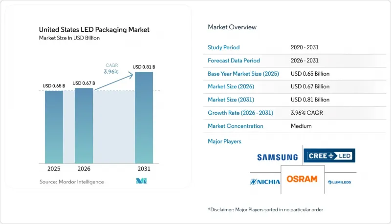
United States LED Packaging - Market Share Analysis, Industry Trends & Statistics, Growth Forecasts (2026 - 2031)
According to Mordor Intelligence, the united states lED packaging market size was valued at USD 0.65 billion in 2025 and estimated to grow from USD 0.67 billion in 2026 to reach USD 0.81 billion by 2031, at a CAGR of 3.96% during the forecast period 2026-2031.
This report is Segmented by Packaging Architecture (SMD, COB, CSP, Flip-Chip, DIP, and More), Power Class (Low Power, Mid Power, and More), Emission Type (Visible LED Packages, and More), Material Chemistry (Substrates, Encapsulation, and More), and Application (General Lighting, Automotive Lighting, Display and Backlighting, and More). The Market Forecasts are Provided in Terms of Value (USD).
United States LED Packaging Market Trends and Insights
Surge In Mini-LED Backlight Adoption
Samsung and LG introduced RGB Mini-LED televisions featuring more than 1,000 dimming zones, tripling the LED count versus legacy edge-lit designs. The finer pitch demands chip scale packages under 1 mm2, automated pick-and-place tools exceeding 100,000 units per hour, and enhanced thermal vias to keep junction temperatures below 85 °C, preserving color stability over product lifetimes. Supply-chain learning curves have lowered average Mini-LED TV prices by nearly 30% over the past year, moving the technology from premium to mid-tier segments. For LED packagers, the architecture lifts revenue per panel because discrete red, green, and blue dies replace white LEDs plus quantum-dot films. Demand is strongest in consumer electronics assembly hubs in California and Texas, where rapid design cycles favor domestic suppliers capable of short lead times. The shift also stimulates investment in low-warpage metal-core printed circuit boards that dissipate hotspot heat in high-pixel-density arrays.
Tightening U.S. Energy-Efficiency Norms For Solid-State Lighting
The U.S. Department of Energy finalized a rule in April 2024 that raises general service lamp efficacy to roughly 120 lm W-1 by July 2028, effectively eliminating most non-LED technologies. LED packagers must therefore improve phosphor conversion efficiency and adopt low-thermal-resistance flip-chip designs that sustain high drive currents without color shift. Integrated lamps must now meet power-factor thresholds of 0.7 or higher, linking package thermal design with electronic driver performance. High-CRI and color-tunable products face steeper optimization trade-offs, prompting segmented product lines that separate compliance-focused models from premium human-centric lighting offerings. Over the long term, the rule supports a steady baseline of replacement demand, cushioning the LED packaging market against cyclical swings in new-construction spending.
High Initial Capex For Advanced Packaging Lines
Setting up flip-chip bonding, chip scale package assembly, and automated optical inspection requires investments of USD 30 million to USD 80 million per site. Tool lead times often exceed 12 months, and only a handful of global vendors supply eutectic die-attach ovens, wafer-level phosphor coaters, and sub-0.2 mm pick-and-place systems. Although the CHIPS for America program awarded USD 1.4 billion for advanced-packaging pilot lines, first commercial volumes will serve high-margin microelectronics long before LED products. Many regional packagers therefore outsource critical steps to subcontractors in East Asia, incurring logistics costs and exposure to tariff swings. Access to affordable capital remains the primary barrier for smaller U.S. entrants wishing to target high-reliability automotive or horticulture niches.
Other drivers and restraints analyzed in the detailed report include:
- Rapid Automotive LED Penetration In ADAS Sensors
- Expansion Of Horticulture Lighting In Controlled-Environment Farming
- IP Litigation Risks Around Flip-Chip Processes
For complete list of drivers and restraints, kindly check the Table Of Contents.
Segment Analysis
Chip scale packages account for the fastest growth trajectory, expanding at a 4.44% CAGR, as television makers and automotive OEMs demand sub-millimeter footprints that reduce optical losses and simplify assembly. Surface mount device formats still delivered the largest 41.38% LED packaging market share in 2025, supported by broad availability and well-established pick-and-place infrastructure.
The migration toward fine-pitch Mini-LED backlights and pixelated headlights is elevating interest in flip-chip architectures that eliminate top-side electrodes, trimming junction-to-case thermal resistance by up to 40%. Meanwhile, chip-on-board modules retain relevance in commercial downlights and horticulture fixtures where continuous high flux and uniform color output matter. Dual in-line and through-hole packages persist in retrofit signage but face erosion as automated surface-mount processes dominate. Integrated matrix device and glass-on-board concepts within the LED packaging market are emerging to co-package driver ICs, thermal spreaders, and optics for highly integrated displays, signaling a convergence of semiconductor and printed-circuit manufacturing disciplines.
Mid-power devices held 36.83% of the United States LED packaging market in 2025 value because they satisfy typical A-lamp and troffer requirements at modest cost, yet tightening efficacy rules favor consolidation into fewer, brighter packages. High-power modules (1-3 W) are therefore projected to outpace the overall LED packaging market size with a 4.21% CAGR, fueled by street-lighting retrofits, horticulture luminaires, and adaptive automotive beams that require sustained luminous flux.
Ultra-high-power units above 3 W confront thermal flux densities near 85 W cm-2, compelling adoption of aluminum-nitride ceramics, vapor-chamber heat spreaders, and active cooling strategies. At the opposite end, low-power indicators lose relevance in general service lamps as minimum lumen thresholds rise. Rising drive currents are also directing R&D dollars toward high-reliability silver-sintered die attach and high-thermal-conductivity phosphor-silicone composites, maintaining performance even when junctions surpass 100 °C during automotive or horticultural duty cycles.
List of Companies Covered in this Report:
- Wolfspeed Inc.
- Lumileds Holding B.V.
- Nichia Corporation
- Osram Opto Semiconductors GmbH
- Samsung Electronics Co., Ltd. (Samsung LED)
- Seoul Semiconductor Co., Ltd.
- LG Innotek Co., Ltd.
- Everlight Electronics Co., Ltd.
- Bridgelux Inc.
- Cree LED, an SGH Company
- Lite-On Technology Corporation
- Stanley Electric Co., Ltd.
- Citizen Electronics Co., Ltd.
- Epistar Corporation
- Lextar Electronics Corporation
- Dominant Opto Technologies Sdn. Bhd.
- Advanced Optoelectronic Technology Inc.
- Unity Opto Technology Co., Ltd.
- Huga Optotech Inc.
- Acuity Brands Lighting Inc.
Additional Benefits:
- The market estimate (ME) sheet in Excel format
- 3 months of analyst support
TABLE OF CONTENTS
1 INTRODUCTION
- 1.1 Study Assumptions, Market Definition
- 1.2 Scope of the Study
2 RESEARCH METHODOLOGY
3 EXECUTIVE SUMMARY
4 MARKET LANDSCAPE
- 4.1 Market Overview
- 4.2 Industry Value-Chain Analysis
- 4.3 Technology Analysis
- 4.4 Regulatory Landscape
- 4.5 Impact of Macroeconomic Factors on the Market
- 4.6 Market Drivers
- 4.6.1 Surge in Mini-LED Backlight Adoption
- 4.6.2 Tightening U.S. Energy-Efficiency Norms for Solid-State Lighting
- 4.6.3 Rapid Automotive LED Penetration in ADAS Sensors
- 4.6.4 Expansion of Horticulture Lighting in Controlled-Environment Farming
- 4.6.5 Government On-shoring Incentives for Semiconductor Packaging
- 4.6.6 Breakthroughs in Silicon Photonics Integrated Packaging
- 4.7 Market Restraints
- 4.7.1 High Initial Capex for Advanced Packaging Lines
- 4.7.2 IP Litigation Risks Around Flip-Chip Processes
- 4.7.3 Volatility in Phosphor Rare-Earth Supply Chain
- 4.7.4 Thermal-Management Challenges at Ultra-High Power Levels
- 4.8 Porter's Five Forces Analysis
- 4.8.1 Bargaining Power of Suppliers
- 4.8.2 Bargaining Power of Buyers
- 4.8.3 Threat of New Entrants
- 4.8.4 Threat of Substitutes
- 4.8.5 Intensity of Competitive Rivalry
5 MARKET SIZE AND GROWTH FORECASTS (VALUE)
- 5.1 By Packaging Architecture
- 5.1.1 Surface Mount Device (SMD)
- 5.1.2 Chip-on-Board (COB)
- 5.1.3 Chip Scale Package (CSP)
- 5.1.4 Flip-Chip LED Packages
- 5.1.5 Dual In-line Package (DIP / Through-hole)
- 5.1.6 Others - IMD, GOB, Mini-LED Display Packaging
- 5.2 By Power Class
- 5.2.1 Low Power (Less Than 0.5 W)
- 5.2.2 Mid Power (0.5 to 1 W)
- 5.2.3 High Power (1 to 3 W)
- 5.2.4 Ultra-High Power (More Than 3 W)
- 5.3 By Emission Type
- 5.3.1 Visible LED Packages
- 5.3.2 Infrared (IR) LED Packages
- 5.3.3 Ultraviolet (UV) LED Packages
- 5.4 By Material Chemistry
- 5.4.1 Substrates
- 5.4.2 Encapsulation
- 5.4.3 Bonding / Die-Attach
- 5.4.4 Phosphors / Coatings
- 5.5 By Application
- 5.5.1 General Lighting
- 5.5.2 Automotive Lighting
- 5.5.3 Display and Backlighting
- 5.5.4 Consumer Electronics
- 5.5.5 Industrial and Specialty
6 COMPETITIVE LANDSCAPE
- 6.1 Market Concentration Analysis
- 6.2 Strategic Moves
- 6.3 Market Share Analysis
- 6.4 Company Profiles (includes Global Level Overview, Market Level Overview, Core Segments, Financials as available, Strategic Information, Market Rank/Share, Products and Services, Recent Developments)
- 6.4.1 Wolfspeed Inc.
- 6.4.2 Lumileds Holding B.V.
- 6.4.3 Nichia Corporation
- 6.4.4 Osram Opto Semiconductors GmbH
- 6.4.5 Samsung Electronics Co., Ltd. (Samsung LED)
- 6.4.6 Seoul Semiconductor Co., Ltd.
- 6.4.7 LG Innotek Co., Ltd.
- 6.4.8 Everlight Electronics Co., Ltd.
- 6.4.9 Bridgelux Inc.
- 6.4.10 Cree LED, an SGH Company
- 6.4.11 Lite-On Technology Corporation
- 6.4.12 Stanley Electric Co., Ltd.
- 6.4.13 Citizen Electronics Co., Ltd.
- 6.4.14 Epistar Corporation
- 6.4.15 Lextar Electronics Corporation
- 6.4.16 Dominant Opto Technologies Sdn. Bhd.
- 6.4.17 Advanced Optoelectronic Technology Inc.
- 6.4.18 Unity Opto Technology Co., Ltd.
- 6.4.19 Huga Optotech Inc.
- 6.4.20 Acuity Brands Lighting Inc.
7 MARKET OPPORTUNITIES AND FUTURE OUTLOOK
- 7.1 White-Space and Unmet-Need Assessment

