PUBLISHER: Mordor Intelligence | PRODUCT CODE: 2119206

PUBLISHER: Mordor Intelligence | PRODUCT CODE: 2119206
United States Semiconductor Manufacturing Equipment - Market Share Analysis, Industry Trends & Statistics, Growth Forecasts (2026 - 2031)
According to Mordor Intelligence, the United States semiconductor manufacturing equipment market was valued at USD 12.89 billion in 2025 and estimated to grow from USD 14.44 billion in 2026 to reach USD 24.83 billion by 2031, at a CAGR of 11.4% during the forecast period (2026-2031).
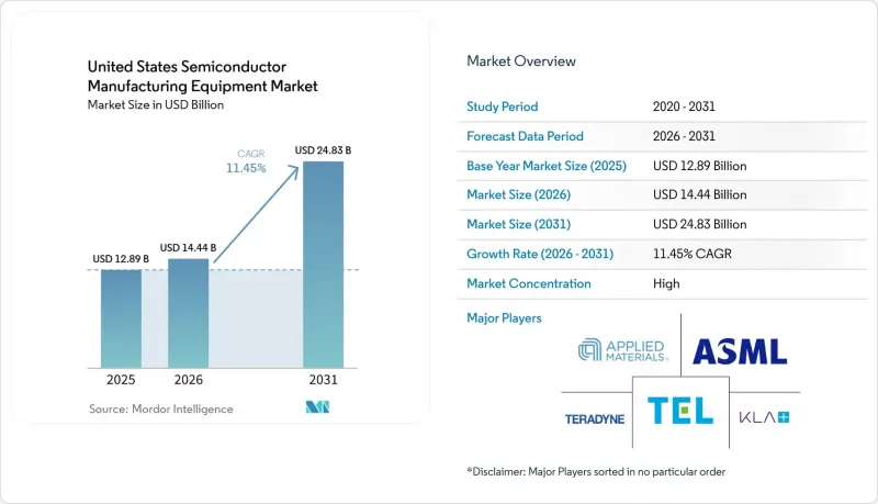
Domestic fabrication projects are shifting from construction to equipment installation, which is expected to increase demand for wafer processing, packaging, testing, and factory support tools. This report is Segmented by Equipment Type (Front-End Equipment, Assembly & Packaging Equipment, Test Equipment, Fab Facility & Support Equipment), by Device Type (Logic and Microcomponents, Memory, Microprocessors, Analog, and More), and by End User (Integrated Device Manufacturers, Foundries, Osats, Others). The Market Forecasts are Provided in Terms of Value (USD).
United States Semiconductor Manufacturing Equipment Market Trends and Insights
CHIPS Act Incentives and Domestic Fab Buildout
The CHIPS and Science Act provides USD 39 billion in direct manufacturing incentives and USD 11 billion for research and development infrastructure. By January 2025, 19 companies had received USD 30.7 billion in awards and USD 5.5 billion in loans for 40 commercial fabrication projects. The 35% investment tax credit applies to eligible projects that begin construction before December 31, 2026, thereby supporting earlier equipment ordering. TSMC has committed USD 265 billion for 12 fabrication and packaging facilities in Arizona. Texas Instruments plans to invest more than USD 60 billion across 7 United States fabs in Texas and Utah.
AI and High-Performance Computing Capacity Expansion
AI data centers require more leading-edge logic, higher-bandwidth memory, and greater advanced packaging capacity. The Semiconductor Industry Association projected a 56.3% CAGR for the AI data center ecosystem from 2025 through 2028. SEMI expects global 300mm fab equipment spending to reach USD 142 billion in 2026, rising 25% from the prior year, with logic and memory capacity supporting the increase. Wafer-processing equipment for front-end AI chip production grew 12% in 2025, while test equipment billings increased 55%. Leading-edge logic, DRAM, and advanced packaging accounted for more than 80% of incremental wafer-fab equipment spending in 2026. This concentrates opportunities among suppliers with exposure to those production areas, rather than in demand for mature nodes or legacy equipment.
Extreme Capital Intensity and Long Tool Payback Periods
A leading-edge 2nm fab requires USD 18 billion-USD 25 billion in total capital expenditure, with equipment accounting for 80% of that amount. Mature-node projects still require substantial investment, with a 28nm-65nm fab averaging USD 4.5 billion in capital expenditure. SEMI expects global 300mm fab equipment spending to total USD 374 billion during 2026-2028. Tool payback periods can extend from 5 to 8 years, depending on yields and utilization. The cost of construction and operation in the United States remains higher than in major Asian manufacturing locations. These conditions make financing, incentive terms, skilled service labor, and reliable supplies of specialized components important to equipment purchasing schedules.
Other drivers and restraints analyzed in the detailed report include:
- Advanced-Node Scaling and Equipment Intensity
- Advanced Packaging, Resilience, and Research Capacity
- Export Controls and Compliance Complexity
For complete list of drivers and restraints, kindly check the Table Of Contents.
Segment Analysis
Front-end equipment represented the largest equipment category in the United States semiconductor manufacturing equipment market in 2025, accounting for 64.0% of market revenue. Lithography, deposition, etching, cleaning, chemical mechanical planarization, thermal processing, and metrology are required throughout the wafer production flow. Gate-all-around structures at 2nm require atomic-layer deposition, selective etching, and gate-dielectric steps that older FinFET tool fleets cannot fully support. More process steps per wafer increase demand for chambers, consumables, and inspection touchpoints. ASML is increasing EUV and DUV production capacity by 30% annually during the next 2 years to address customer demand. Applied Materials has stated that deposition and etch are growing faster than lithography at 2nm because the transition raises materials intensity.
Assembly and packaging equipment was the fastest-growing equipment category, supported by heterogeneous integration. Wire-bonding and flip-chip systems continue to support mature-node analog, power, and automotive devices. CoWoS, hybrid bonding, and wafer-level fan-out require more specialized equipment for AI accelerators. TSMC's target of 50,000 SoIC wafers per month by 2027 would require additional die-attach and hybrid-bonding tools. Test equipment billings increased 55% in 2025 as AI chips and stacked high-bandwidth memory required more validation. Factory automation, chemical and gas delivery, and cleanroom systems also benefit from greenfield projects in the United States, where facilities are designed around newer automation architectures. The United States semiconductor manufacturing equipment industry also requires support tools that allow new plants to manage material movement and process utilities from the start.
Complete Report Scope:
- By Equipment Type
- Wafer Fab Equipment / Front-End Equipment (lithography, deposition, etching, cleaning, CMP, thermal processing, front-end metrology & inspection equipment, etc.)
- Assembly and Packaging Equipment (die attach, wire bonding, flip-chip bonding, wafer bumping, thinning, dicing, molding, etc.)
- Semiconductor Test Equipment (automated test equipment, wafer probers, test handlers, burn-in equipment, and final test equipment)
- Fab Facility, Automation and Support Equipment (automation systems, wafer handling systems, AMHS, chemical & gas delivery systems, chillers, cleanroom support equipment, etc.)
- By Device Type
- Logic and Microcomponents (logic ICs, microprocessors, etc.)
- Memory (DRAM, NAND, HBM, NOR, etc.)
- Microprocessors (MPUs)
- Analog (Power management ICs, signal chain, interface Ics, etc.)
- Discrete and Power Devices (Diodes, transistors, MOSFETs, etc.)
- Sensors, MEMS and Optoelectronic Devices (Image sensors, MEMS sensors, etc.)
- By End User
- Integrated Device Manufacturers (IDMs)
- Foundries
- Outsourced Semiconductor Assembly and Test (OSAT) Companies
- Others (Research & Development (R&D) and Pilot Lines)
List of Companies Covered in this Report:
- Applied Materials, Inc.
- ASML Holding N.V.
- Lam Research Corporation
- Tokyo Electron Limited
- KLA Corporation
- SCREEN Holdings Co., Ltd.
- Teradyne, Inc.
- Advantest Corporation
- Hitachi High-Tech Corporation
- Plasma-Therm LLC
- ASM International N.V.
- Veeco Instruments Inc.
- Onto Innovation Inc.
- Nova Ltd.
- Cohu, Inc.
- FormFactor, Inc.
- Kulicke and Soffa Industries, Inc.
- BE Semiconductor Industries N.V.
- EV Group
- Nordson Corporation
- ACM Research, Inc.
- Ferrotec Holdings Corporation
- Modutek Corporation
Additional Benefits:
- The market estimate (ME) sheet in Excel format
- 3 months of analyst support
TABLE OF CONTENTS
1 INTRODUCTION
- 1.1 Study Assumptions and Market Definition
- 1.2 Scope of the Study
2 RESEARCH METHODOLOGY
3 EXECUTIVE SUMMARY
4 MARKET LANDSCAPE
- 4.1 Market Overview
- 4.2 Market Drivers
- 4.2.1 CHIPS Act Incentives and Domestic Fab Buildout
- 4.2.2 AI and High-Performance Computing Capacity Expansion
- 4.2.3 Advanced-Node Scaling and Greater Equipment Intensity per Wafer
- 4.2.4 Advanced Packaging and Heterogeneous Integration Adoption
- 4.2.5 Domestic Supply-Chain Resilience and National-Security Procurement
- 4.2.6 High-NA EUV Ecosystem Development in Albany and Other Research Hubs
- 4.3 Market Restraints
- 4.3.1 Extreme Capital Intensity and Long Tool Payback Periods
- 4.3.2 Skilled Field-Service Engineer Shortage
- 4.3.3 Export Controls and Cross-Border Compliance Complexity
- 4.3.4 Domestic Shortages of Semiconductor-Grade Components and Consumables
- 4.4 Value and Supply-Chain Analysis
- 4.4.1 Supply Chain Localization and Strategic Investments by Leading Semiconductor Manufacturers
- 4.5 Regulatory and Policy Landscape
- 4.6 Technology and Innovation Trends
- 4.6.1 Technology Leadership in Advanced Process Nodes and Next-Generation Manufacturing
- 4.6.2 Expansion of Domestic Semiconductor Manufacturing Capacity
- 4.6.3 CHIPS and Science Act Driving Fab Investments and Equipment Demand
- 4.6.4 Increasing Demand for Wafer Fabrication, Advanced Packaging, and Process Control Equipment
- 4.7 Impact Assessment of Geopolitical Events on the Market
5 MARKET SIZE AND GROWTH FORECASTS
- 5.1 By Equipment Type
- 5.1.1 Wafer Fab Equipment / Front-End Equipment (lithography, deposition, etching, cleaning, CMP, thermal processing, front-end metrology & inspection equipment, etc.)
- 5.1.2 Assembly and Packaging Equipment (die attach, wire bonding, flip-chip bonding, wafer bumping, thinning, dicing, molding, etc.)
- 5.1.3 Semiconductor Test Equipment (automated test equipment, wafer probers, test handlers, burn-in equipment, and final test equipment)
- 5.1.4 Fab Facility, Automation and Support Equipment (automation systems, wafer handling systems, AMHS, chemical & gas delivery systems, chillers, cleanroom support equipment, etc.)
- 5.2 By Device Type
- 5.2.1 Logic and Microcomponents (logic ICs, microprocessors, etc.)
- 5.2.2 Memory (DRAM, NAND, HBM, NOR, etc.)
- 5.2.3 Microprocessors (MPUs)
- 5.2.4 Analog (Power management ICs, signal chain, interface Ics, etc.)
- 5.2.5 Discrete and Power Devices (Diodes, transistors, MOSFETs, etc.)
- 5.2.6 Sensors, MEMS and Optoelectronic Devices (Image sensors, MEMS sensors, etc.)
- 5.3 By End User
- 5.3.1 Integrated Device Manufacturers (IDMs)
- 5.3.2 Foundries
- 5.3.3 Outsourced Semiconductor Assembly and Test (OSAT) Companies
- 5.3.4 Others (Research & Development (R&D) and Pilot Lines)
6 COMPETITIVE LANDSCAPE
- 6.1 Market Concentration
- 6.2 Strategic Moves
- 6.2.1 Product Launches and Technology Upgrades
- 6.2.2 Capacity Expansion and U.S. Localization
- 6.2.3 Partnerships, Alliances, and Customer Co-Development
- 6.2.4 Acquisitions and Portfolio Expansion
- 6.3 Market Share Analysis
- 6.4 Company Profiles (includes Global Level Overview, Market Level Overview, Core Segments, Financials as available, Strategic Information, Products and Services, Recent Developments)
- 6.4.1 Applied Materials, Inc.
- 6.4.2 ASML Holding N.V.
- 6.4.3 Lam Research Corporation
- 6.4.4 Tokyo Electron Limited
- 6.4.5 KLA Corporation
- 6.4.6 SCREEN Holdings Co., Ltd.
- 6.4.7 Teradyne, Inc.
- 6.4.8 Advantest Corporation
- 6.4.9 Hitachi High-Tech Corporation
- 6.4.10 Plasma-Therm LLC
- 6.4.11 ASM International N.V.
- 6.4.12 Veeco Instruments Inc.
- 6.4.13 Onto Innovation Inc.
- 6.4.14 Nova Ltd.
- 6.4.15 Cohu, Inc.
- 6.4.16 FormFactor, Inc.
- 6.4.17 Kulicke and Soffa Industries, Inc.
- 6.4.18 BE Semiconductor Industries N.V.
- 6.4.19 EV Group
- 6.4.20 Nordson Corporation
- 6.4.21 ACM Research, Inc.
- 6.4.22 Ferrotec Holdings Corporation
- 6.4.23 Modutek Corporation
7 MARKET OPPORTUNITIES AND FUTURE OUTLOOK
- 7.1 White-Space and Unmet-Need Assessment
- 7.2 Future Outlook

