
PUBLISHER: Mordor Intelligence | PRODUCT CODE: 2043999

PUBLISHER: Mordor Intelligence | PRODUCT CODE: 2043999
Japan Semiconductor Silicon Wafer - Market Share Analysis, Industry Trends & Statistics, Growth Forecasts (2026 - 2031)
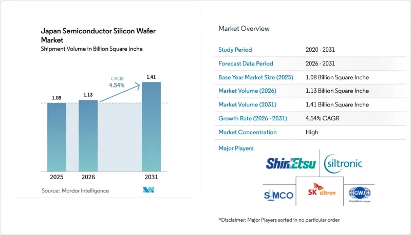
The Japan Semiconductor Silicon Wafer Market size in terms of shipment volume is expected to increase from 1.08 Billion Square Inche in 2025 to 1.13 Billion Square Inche in 2026 and reach 1.41 Billion Square Inche by 2031, growing at a CAGR of 4.54% over 2026-2031.
Policy makers have placed upstream materials at the center of the country's re-shoring push, tying multi-year subsidies to local wafer output, advanced packaging, and 2-nanometer logic readiness. Demand is clustering around 300 millimeter substrates as new logic and high-bandwidth memory lines ramp, while specialty silicon gains traction in automotive and radio-frequency designs. Large incumbents maintain scale advantages, yet rising power tariffs and strict wastewater rules compress margins and open niches for agile specialty-wafer suppliers. Talent shortages and smartphone cyclicality remain the main near-term brakes, but long-duration automotive contracts and domestic mega-fab expansions underpin the medium-term growth outlook for the Japan semiconductor silicon wafer market.
Japan Semiconductor Silicon Wafer Market Trends and Insights
Rising Demand For 300 mm Wafers In Logic And Memory Devices
Shipments of 300-millimeter substrates grew 5.8% year on year in 2025 as artificial-intelligence accelerators and sub-16-nanometer logic scaled up volume. The first Kumamoto line alone pulls roughly 55,000 wafers each month, and its phase-two expansion adds another 50,000 by late 2027, lifting domestic demand by more than 1.2 million wafers annually. Parallel node migrations in DRAM and NAND eliminate the cost advantage of 200 millimeter tools, intensifying the swing toward larger diameters. Crystal-growth equipment lead times hover at 18 months, delaying supply responses and preserving tight market conditions. This driver, therefore, anchors mid-term growth for the Japan semiconductor silicon wafer market.
Government Subsidies For Domestic Wafer Capacity Expansion
The Ministry of Economy, Trade and Industry budgeted JPY 1.23 trillion (USD 8.7 billion) for semiconductor infrastructure in fiscal 2026, with JPY 400 billion (USD 2.8 billion) ring-fenced for wafer lines, epitaxial tools, and materials R and D. Funding agreements oblige suppliers to hit domestic employment and technology-transfer targets, ensuring near-term installation of an additional 300 millimeter pullers and epitaxial reactors. Shin-Etsu and SUMCO together secured JPY 95 billion (USD 670 million) to lift capacity by 15% through 2027, while midsize firms accessed smaller grants for specialty silicon. The front-loaded nature of disbursements gives the Japan semiconductor silicon wafer market an immediate volume boost and offsets the capital intensity of environmental compliance.
Prolonged Downturn In Global Smartphone Demand
Three consecutive quarters of shipment contraction in early 2025 cut high-margin logic-wafer exports to overseas foundries. Shin-Etsu idled two pullers and deferred a JPY 30 billion (USD 210 million) expansion, while SUMCO trimmed revenue guidance by 7% . Because smartphone processors and NAND controllers require tight flatness and low contamination, the lost orders carry outsized profitability. Recovery hinges on 5 G penetration in price-sensitive markets, leaving a near-term hole in utilization rates for the Japan semiconductor silicon wafer market.
Other drivers and restraints analyzed in the detailed report include:
- Kumamoto Mega-Fab Build-out By TSMC-Sony JV
- Accelerated Electrification Of Japanese Automotive Industry
- High Electricity Costs Affecting Manufacturing Competitiveness
For complete list of drivers and restraints, kindly check the Table Of Contents.
Segment Analysis
The 300 millimeter category dominated the Japan semiconductor silicon wafer market size with a 71.28% volume share in 2025 and continues to outgrow smaller diameters at a 4.95% CAGR. Node migrations below 16 nanometers and high-bandwidth memory stacking make large-area substrates essential for cost amortization, and the Kumamoto and Hokkaido fabs together will require more than 2 million wafers annually by 2028. Tight supply directs capital toward new Czochralski pullers and advanced polishing lines, yet 18-month tool lead times delay relief until mid-2027.
Conversely, the 200 millimeter segment retains an entrenched role in analog, power and microcontroller production that favors proven process recipes over die density. Automotive electrification, industrial automation and sensor demand keep 200 millimeter fabs running near full utilization, even as equipment suppliers wind down spare-parts support. Diameters up to 150 millimeters remain niche at roughly 5% of volume, serving prototyping and specialty RF devices where quick cycle times trump economies of scale. This mixed outlook means the Japan semiconductor silicon wafer market share for 300 millimeter substrates will keep inching upward, while volumes for smaller diameters hold steady rather than fall.
Logic devices captured 36.29% of Japan's semiconductor silicon wafer market share in 2025, with expansion set at a 5.05% CAGR as 3-nanometer production localizes. Rapidus adds diversification by introducing 2-nanometer capacity in Hokkaido after 2027, anchoring additional wafer pull in northern Japan. Memory follows at 4.6% CAGR, buoyed by artificial-intelligence servers that integrate high-bandwidth DRAM stacks and dense NAND for edge storage.
Analog demand grows steadily across multi-year industrial and telecom design cycles, whereas discrete devices pivot toward silicon carbide and gallium nitride for high-voltage automotive inverters. Specialty categories such as sensors and optoelectronics accelerate alongside lidar and time-of-flight adoption in advanced driver-assistance systems. This balanced mix cushions the Japan semiconductor silicon wafer market against single-segment shocks and underscores the strategic value of maintaining breadth across device families.
The Japan Semiconductor Silicon Wafer Market Report is Segmented by Wafer Diameter (Up To 150 Mm, 200 Mm, and 300 Mm), Semiconductor Device Type (Logic, Memory, Analog, and More), Wafer Type (Prime Polished, Epitaxial, Silicon-On-Insulator (SOI), and More), End-User (Consumer Electronics, Mobile and Smartphones, Pcs and Servers, and More), and Country. The Market Forecasts are Provided in Terms of Volume (Square Inches).
List of Companies Covered in this Report:
- Shin-Etsu Chemical Co., Ltd.
- SUMCO Corporation
- GlobalWafers Japan Co., Ltd.
- Siltronic AG
- SK Siltron Co., Ltd.
- Okmetic Oy
- Wafer Works Corporation
- Ferrotec Holdings Corporation
- Mitsubishi Materials Corporation
- Tokuyama Corporation
- Resonac Holdings Corporation
- National Silicon Industry Group (NSIG)
- Hebei Zhonghuan Semiconductor Co., Ltd.
- Topsil GlobalWafers A/S
- Soitec SA
- SEH America, Inc.
- MEMC Electronic Materials, Inc.
- Elkem ASA
- Shanghai Advanced Silicon Technology Co., Ltd.
- Siltronic Japan Corp.
Additional Benefits:
- The market estimate (ME) sheet in Excel format
- 3 months of analyst support
TABLE OF CONTENTS
1 INTRODUCTION
- 1.1 Study Assumptions and Market Definition
- 1.2 Scope of the Study
2 RESEARCH METHODOLOGY
3 EXECUTIVE SUMMARY
4 MARKET LANDSCAPE
- 4.1 Market Overview
- 4.2 Industry Value-Chain Analysis
- 4.3 Technology Analysis
- 4.4 Regulatory Landscape
- 4.5 Impact of Macroeconomic Factors
- 4.6 Market Drivers
- 4.6.1 Rising Demand for 300 mm Wafers in Logic and Memory Devices
- 4.6.2 Government Subsidies for Domestic Wafer Capacity Expansion
- 4.6.3 Kumamoto Mega-Fab Build-out by TSMC-Sony JV
- 4.6.4 Accelerated Electrification of Japanese Automotive Industry
- 4.6.5 Supply-Chain Re-Shoring Initiatives among IDMs
- 4.6.6 Breakthrough in Float-Zone-Czochralski Hybrid Crystal Pulling
- 4.7 Market Restraints
- 4.7.1 Prolonged Downturn in Global Smartphone Demand
- 4.7.2 High Electricity Costs Affecting Manufacturing Competitiveness
- 4.7.3 Stringent Waste-Water Regulations on Silicon Processing
- 4.7.4 Engineering Talent Shortage in Crystal Growth Operations
- 4.8 Porter's Five Forces Analysis
- 4.8.1 Bargaining Power of Suppliers
- 4.8.2 Bargaining Power of Buyers
- 4.8.3 Threat of New Entrants
- 4.8.4 Threat of Substitutes
- 4.8.5 Intensity of Competitive Rivalry
5 MARKET SIZE AND GROWTH FORECASTS (VOLUME)
- 5.1 By Wafer Diameter
- 5.1.1 Up to 150 mm
- 5.1.2 200 mm
- 5.1.3 300 mm
- 5.2 By Semiconductor Device Type
- 5.2.1 Logic
- 5.2.2 Memory
- 5.2.3 Analog
- 5.2.4 Discrete
- 5.2.5 Other Semiconductor Device Types (Optoelectronics, Sensors, Micro)
- 5.3 By Wafer Type
- 5.3.1 Prime Polished
- 5.3.2 Epitaxial
- 5.3.3 Silicon-on-Insulator (SOI)
- 5.3.4 Specialty Silicon (High-Resistivity, Power, Sensor-Grade)
- 5.4 By End-User
- 5.4.1 Consumer Electronics
- 5.4.2 Mobile and Smartphones
- 5.4.3 PCs and Servers
- 5.4.4 Industrial
- 5.4.5 Telecommunications
- 5.4.6 Automotive
- 5.4.7 Other End-User
6 COMPETITIVE LANDSCAPE
- 6.1 Market Concentration
- 6.2 Strategic Moves
- 6.3 Market Share Analysis
- 6.4 Company Profiles (includes Global Level Overview, Market Level Overview, Core Segments, Financials as available, Strategic Information, Market Rank/Share, Products and Services, Recent Developments)
- 6.4.1 Shin-Etsu Chemical Co., Ltd.
- 6.4.2 SUMCO Corporation
- 6.4.3 GlobalWafers Japan Co., Ltd.
- 6.4.4 Siltronic AG
- 6.4.5 SK Siltron Co., Ltd.
- 6.4.6 Okmetic Oy
- 6.4.7 Wafer Works Corporation
- 6.4.8 Ferrotec Holdings Corporation
- 6.4.9 Mitsubishi Materials Corporation
- 6.4.10 Tokuyama Corporation
- 6.4.11 Resonac Holdings Corporation
- 6.4.12 National Silicon Industry Group (NSIG)
- 6.4.13 Hebei Zhonghuan Semiconductor Co., Ltd.
- 6.4.14 Topsil GlobalWafers A/S
- 6.4.15 Soitec SA
- 6.4.16 SEH America, Inc.
- 6.4.17 MEMC Electronic Materials, Inc.
- 6.4.18 Elkem ASA
- 6.4.19 Shanghai Advanced Silicon Technology Co., Ltd.
- 6.4.20 Siltronic Japan Corp.
7 MARKET OPPORTUNITIES AND FUTURE OUTLOOK
- 7.1 White-Space and Unmet-Need Assessment

