PUBLISHER: Mordor Intelligence | PRODUCT CODE: 2123331

PUBLISHER: Mordor Intelligence | PRODUCT CODE: 2123331
Semiconductor Equipment - Market Share Analysis, Industry Trends & Statistics, Growth Forecasts (2026 - 2031)
According to Mordor Intelligence, the semiconductor equipment market size is estimated at USD 114.82 billion in 2026, and is expected to reach USD 162.70 billion by 2031, at a CAGR of 7.22% during the forecast period (2026-2031).
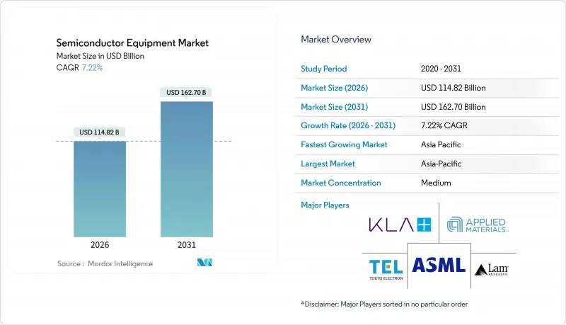
This report is Segmented by Equipment Type (Front-End Equipment and Back-End Equipment), Supply-Chain Participant (Integrated Device Manufacturers, Foundry, and More), Wafer Size (300mm, 200mm, Less Than or Equal To 150mm), End-Use Industry (Computing and Data-Center, Communications, Automotive and Mobility, and More), and Geography. Market Forecasts are Provided in Terms of Value (USD)
Global Semiconductor Equipment Market Trends and Insights
Rapid AI, IoT and Edge-Device Node Investments
Artificial-intelligence inference workloads and distributed edge computing are pushing process nodes below 5 nm, where equipment intensity per wafer rises sharply. OpenAI committed USD 500 million in 2025 to secure advanced-node capacity at Taiwan Semiconductor Manufacturing Company (TSMC), while Microsoft and Amazon Web Services each placed multi-billion-dollar reservations for 3 nm custom silicon. ASML reported a 40% year-on-year increase in EUV tool shipments during the first three quarters of 2025. In contrast, IoT devices stay on mature 28 nm and 40 nm lines, yet emerging edge-AI accelerators combine radio-frequency layers at 22 nm with digital logic at 7 nm, forcing fabs to install heterogeneous packaging lines that merge dissimilar dies. The International Technology Roadmap for Semiconductors projects that by 2028, more than half of high-performance chips will adopt chiplet architectures, each requiring novel assembly, test, and advanced packaging equipment.
Government Subsidy Waves Boosting Tool CAPEX
Legislation such as the United States CHIPS and Science Act and the EU Chips Act compresses procurement cycles that formerly spanned two years. Intel secured USD 8.5 billion in grants plus USD 11 billion in loan guarantees for new fabs in Ohio and Arizona, committing to purchase over 200 leading-edge tools by 2028. Micron, Samsung and Rapidus received similar state support in New York, South Korea and Japan, respectively. India's Ministry of Electronics and Information Technology approved USD 2.75 billion for Micron's Gujarat assembly facility, spurring orders for back-end platforms. These incentives front-load demand into the 2026-2028 window, lifting the semiconductor equipment market yet raising utilization-rate questions once subsidies taper.
Export-Control Restrictions on China-Bound Tools
From September 2025, the Netherlands, the United States, and Japan tightened licensing for lithography, deposition, and etch platforms capable of sub-14 nm patterning, blocking shipments to Chinese fabs. China's equipment imports fell 28% year-on-year in 1H 2025, while local suppliers Advanced Micro-Fabrication Equipment and Naura Technology Group grew 42% as fabs accepted older-generation domestic tools. The split forces Western vendors to concentrate high-end sales in Taiwan, South Korea, and North America, while risking long-term share erosion once Chinese producers close the technology gap.
Other drivers and restraints analyzed in the detailed report include:
- Transition to GAA and High-NA EUV Toolsets
- 3D Heterogeneous-Integration Packaging Demand Spike
- Specialty-Material Supply Bottlenecks Delaying Tool Shipments
For complete list of drivers and restraints, kindly check the Table Of Contents.
Segment Analysis
Front-end platforms captured 70.33% semiconductor equipment market share in 2025 and are tracking an 8.16% CAGR through 2031. Lithography alone accounted for 35% of total outlays in 2025, as fabs migrated from 0.33-NA to 0.55-NA EUV systems priced at over USD 400 million each. Etch revenues climbed 9.2% in the same year because GAA structures require selective removal of sacrificial silicon-germanium. Deposition tools, particularly ALD and CVD, grew 8.7% on 2 nm uptake. Metrology and inspection expanded 10.1% as inline defect detection becomes mandatory below 10 nm.
Back-end tools accounted for 29.67% of the semiconductor equipment market in 2025 and will grow at a 6.8% CAGR. Hybrid-bonding equipment for chiplet assembly rose 11% in 2025, while high-bandwidth-memory testers advanced 14% amid 12-die stack adoption. Cleaning and photoresist processing units each improved 7.4%. Although packaging gains relevance, the capital intensity of leading-edge lithography ensures front-end platforms preserve revenue leadership through 2031.
Foundries absorbed 52.92% of 2025 equipment purchases, underpinned by TSMC's USD 32 billion and Samsung's USD 22 billion capex programs. Integrated device manufacturers (IDMs) followed with 28.24%, dominated by Intel's 18-angstrom and 20-angstrom projects. OSATs held 18.84% but are poised for a 7.84% CAGR as chiplet designs shift complexity toward packaging.
This structure is reshaping supply priorities. Foundries focus on EUV, ALD, and selective-etch, whereas OSATs deploy hybrid-bonding, through-silicon-via, and wafer-level fan-out lines. Rising OSAT capital intensity, from 12% of revenue in 2020 to 16% in 2025, signals a gradual rebalancing of value capture across the semiconductor equipment market.
Complete Report Scope:
- By Equipment Type
- Front-end Equipment
- Lithography Equipment
- Etch Equipment
- Deposition Equipment
- Metrology/Inspection Equipment
- Cleaning Equipment
- Photoresist Processing Equipment
- Other Equipment Types
- Back-end Equipment
- Test Equipment
- Assembly and Packaging Equipment
- Front-end Equipment
- By Supply-Chain Participant
- Integrated Device Manufacturer (IDM)
- Foundry
- Outsourced Semiconductor Assembly and Test (OSAT)
- By Wafer Size
- 300 mm
- 200 mm
- Less than or Equal to 150 mm
- By End-Use Industry
- Computing and Data- Center
- Communications (5G,RF)
- Automotive and Mobility
- Cosumer Electronics
- Industrial and Others
- By Geography
- North America
- United States
- Canada
- Mexico
- South America
- Brazil
- Argentina
- Rest of South America
- Europe
- Germany
- United Kingdom
- France
- Italy
- Spain
- Rest of Europe
- Asia-Pacific
- China
- Japan
- India
- South Korea
- ASEAN
- Rest of Asia-Pacific
- Middle East
- Saudi Arabia
- United Arab Emirates
- Rest of Middle East
- Africa
- South Africa
- Nigeria
- Rest of Africa
- North America
Geography Analysis
Asia-Pacific led the semiconductor equipment market with a 52.97% share in 2025 and is set to post a 9.07% CAGR through 2031. Taiwan alone imported USD 28 billion of tools in 2025 as TSMC installed more than 100 EUV systems across three fabs. South Korea followed with USD 19 billion in spend, split between foundry and memory. Although China's imports dropped from USD 33 billion in 2024 to USD 24 billion in 2025, domestic vendors shipped over 600 units to local fabs, partially offsetting the impact of export controls.
North America accounted for 24.8% of 2025 revenue and will grow at an 8.3% CAGR, accelerated by the CHIPS Act funding that de-risks Intel, Micron, and Texas Instruments expansions. Europe held 18.6% and is advancing at 7.1% as the European Semiconductor Manufacturing Company builds a EUR 10 billion Dresden fab focused on automotive nodes. The Middle East and Africa together captured 2.1%, driven by sovereign diversification programs, while South America's 1.53% share stems mainly from Brazilian assembly lines.
Differences in subsidy structures and geopolitical risk are shaping regional allocations of tools. Allied regions move ahead with high-NA EUV, whereas China prioritizes indigenous 28 nm and 14 nm capacity, reinforcing a bifurcated global landscape within the broader semiconductor equipment market.
- Applied Materials, Inc.
- ASML Holding N.V.
- Tokyo Electron Limited
- Lam Research Corporation
- KLA Corporation
- SCREEN Holdings Co., Ltd.
- Teradyne, Inc.
- Hitachi High-Tech Corporation
- Veeco Instruments Inc.
- ASM International N.V.
- Canon Inc.
- Nikon Corporation
- Onto Innovation Inc.
- Nova Ltd.
- Advantest Corporation
- Hanmi Semiconductor Co., Ltd.
- DISCO Corporation
- BE Semiconductor Industries N.V.
- Kulicke & Soffa Industries, Inc.
- FormFactor, Inc.
- Plasma-Therm LLC
- SUSS MicroTec SE
- Kokusai Electric Corporation
- Advanced Micro-Fabrication Equipment Inc. (AMEC)
- Naura Technology Group Co., Ltd.
Additional Benefits:
- The market estimate (ME) sheet in Excel format
- 3 months of analyst support
TABLE OF CONTENTS
1 INTRODUCTION
- 1.1 Study Assumptions and Market Definition
- 1.2 Scope of the Study
2 RESEARCH METHODOLOGY
3 EXECUTIVE SUMMARY
4 MARKET LANDSCAPE
- 4.1 Market Overview
- 4.2 Market Drivers
- 4.2.1 Surging Demand For Advanced Consumer Electronics And Smartphones
- 4.2.2 Rapid AI-, IoT- And Edge-Device Node Investments
- 4.2.3 Government Subsidy Waves (CHIPS Act, EU Chips Act, Etc.) Boosting Tool Capex
- 4.2.4 Transition To GAA And High-NA EUV Necessitating New Toolsets
- 4.2.5 Sustainability Mandates Driving "Green-Fab" Retrofit Tools
- 4.2.6 3D Heterogeneous-Integration Packaging Demand Spike
- 4.3 Market Restraints
- 4.3.1 Extremely High CAPEX And Long Pay-Back Cycles
- 4.3.2 Specialty-Material Supply Bottlenecks Delaying Tool Shipments
- 4.3.3 Export-Control Restrictions On China-Bound Tools
- 4.3.4 Acute Shortage Of Skilled Field-Service Engineers
- 4.4 Industry Value Chain Analysis
- 4.5 Regulatory Landscape
- 4.6 Technological Outlook
- 4.7 Porter's Five Forces Analysis
- 4.7.1 Bargaining Power of Suppliers
- 4.7.2 Bargaining Power of Buyers
- 4.7.3 Threat of New Entrants
- 4.7.4 Threat of Substitute Products
- 4.7.5 Degree of Competition
5 MARKET SIZE AND GROWTH FORECASTS (VALUE)
- 5.1 By Equipment Type
- 5.1.1 Front-end Equipment
- 5.1.1.1 Lithography Equipment
- 5.1.1.2 Etch Equipment
- 5.1.1.3 Deposition Equipment
- 5.1.1.4 Metrology/Inspection Equipment
- 5.1.1.5 Cleaning Equipment
- 5.1.1.6 Photoresist Processing Equipment
- 5.1.1.7 Other Equipment Types
- 5.1.2 Back-end Equipment
- 5.1.2.1 Test Equipment
- 5.1.2.2 Assembly and Packaging Equipment
- 5.1.1 Front-end Equipment
- 5.2 By Supply-Chain Participant
- 5.2.1 Integrated Device Manufacturer (IDM)
- 5.2.2 Foundry
- 5.2.3 Outsourced Semiconductor Assembly and Test (OSAT)
- 5.3 By Wafer Size
- 5.3.1 300 mm
- 5.3.2 200 mm
- 5.3.3 Less than or Equal to 150 mm
- 5.4 By End-Use Industry
- 5.4.1 Computing and Data- Center
- 5.4.2 Communications (5G,RF)
- 5.4.3 Automotive and Mobility
- 5.4.4 Cosumer Electronics
- 5.4.5 Industrial and Others
- 5.5 By Geography
- 5.5.1 North America
- 5.5.1.1 United States
- 5.5.1.2 Canada
- 5.5.1.3 Mexico
- 5.5.2 South America
- 5.5.2.1 Brazil
- 5.5.2.2 Argentina
- 5.5.2.3 Rest of South America
- 5.5.3 Europe
- 5.5.3.1 Germany
- 5.5.3.2 United Kingdom
- 5.5.3.3 France
- 5.5.3.4 Italy
- 5.5.3.5 Spain
- 5.5.3.6 Rest of Europe
- 5.5.4 Asia-Pacific
- 5.5.4.1 China
- 5.5.4.2 Japan
- 5.5.4.3 India
- 5.5.4.4 South Korea
- 5.5.4.5 ASEAN
- 5.5.4.6 Rest of Asia-Pacific
- 5.5.5 Middle East
- 5.5.5.1 Saudi Arabia
- 5.5.5.2 United Arab Emirates
- 5.5.5.3 Rest of Middle East
- 5.5.6 Africa
- 5.5.6.1 South Africa
- 5.5.6.2 Nigeria
- 5.5.6.3 Rest of Africa
- 5.5.1 North America
6 COMPETITIVE LANDSCAPE
- 6.1 Market Concentration
- 6.2 Strategic Moves
- 6.3 Market Share Analysis
- 6.4 Company Profiles (includes Global-level Overview, Market-level Overview, Core Segments, Financials as available, Strategic Information, Market Rank/Share, Products & Services, Recent Developments)
- 6.4.1 Applied Materials, Inc.
- 6.4.2 ASML Holding N.V.
- 6.4.3 Tokyo Electron Limited
- 6.4.4 Lam Research Corporation
- 6.4.5 KLA Corporation
- 6.4.6 SCREEN Holdings Co., Ltd.
- 6.4.7 Teradyne, Inc.
- 6.4.8 Hitachi High-Tech Corporation
- 6.4.9 Veeco Instruments Inc.
- 6.4.10 ASM International N.V.
- 6.4.11 Canon Inc.
- 6.4.12 Nikon Corporation
- 6.4.13 Onto Innovation Inc.
- 6.4.14 Nova Ltd.
- 6.4.15 Advantest Corporation
- 6.4.16 Hanmi Semiconductor Co., Ltd.
- 6.4.17 DISCO Corporation
- 6.4.18 BE Semiconductor Industries N.V.
- 6.4.19 Kulicke & Soffa Industries, Inc.
- 6.4.20 FormFactor, Inc.
- 6.4.21 Plasma-Therm LLC
- 6.4.22 SUSS MicroTec SE
- 6.4.23 Kokusai Electric Corporation
- 6.4.24 Advanced Micro-Fabrication Equipment Inc. (AMEC)
- 6.4.25 Naura Technology Group Co., Ltd.
7 MARKET OPPORTUNITIES AND FUTURE OUTLOOK
- 7.1 White-space and Unmet-need Assessment

